background image

DVR-3100-S

129

5

6

7

8

5

6

7

8

C

D

F

A

B

E

New functions and specifications

In this model, the following new functions and specifications 
have been included in addition to those of conventional models:

1. Improved multitasking functions

This model supports DVD multitasking (only in VR mode), 
which was impossible with conventional models.

a

 Pursuit playback

Playback of the title being recorded by the DVD drive in VR 
mode .

b

 Simultaneous recording/playback 

Playback of a title other than that being recorded by the DVD 
drive in VR mode.

2. Advanced disc NAVI

In the conventional disc NAVI function, recorded titles are 
displayed with still pictures as a list. In the advanced disc 
NAVI function, the title selected with the cursor is displayed 
as an animated picture with sound.

3. Improved Still Picture menu in Video mode

The disc NAVI function, which enables displaying a list of 
recorded titles with still pictures, is enabled in Video mode 
with this model. Selection from among nine title menus is also 
supported.

4. Adoption of MPEG2 SIF

In MN1-6 modes, MPEG2 SIF has been adopted, instead of the 
MPEG1 SIF of conventional models. This enables higher-quality 
recording for longer hours.

5. Improved editing functions

For DVD, the original/play-list editing in DVD-VR mode 
available with conventional models is provided.
The automatic-chapter-mark-insertion function in response to a 
change in audio type (stereo, monaural, bilingual) makes 
commercial-cutting editing easier.

5. Various-format playback

Playback of WMA, MP3, and JPEG formats is supported.

6. Other functions and specifications

The following main functions and specifications adopted with 
conventional models are also provided with this model:
• 192-kHz, 24-bit DAC
• 48-kHz, 20-bit ADC
• Digital 3-D Y/C separation circuit
• Digital frame TBC
• 3-D DNR
• DV (iLink) input/output
• Built-in BS tuner
• Playback with commercials skipped

• CD/video-CD playback
• Picture creation
• Recording with 3/4-D1 and 2/3-D1 resolutions
• Recording mode with 32-step MNs
• LPCM recording
• High-resolution GUI
• Progressive output
• SRS TruSurround

www. xiaoyu163. com

QQ 376315150

9

9

2

8

9

4

2

9

8

TEL 13942296513

9

9

2

8

9

4

2

9

8

0

5

1

5

1

3

6

7

3

Q

Q

TEL  13942296513  QQ  376315150  892498299 

TEL  13942296513  QQ  376315150  892498299 

http://www.xiaoyu163.com

http://www.xiaoyu163.com

Summary of Contents for dvr-3100-s

Page 1: ...VR 3100 S WYXU AC220 240V 2 PG DVR 3100 S WVXU AC220 240V 2 PG When servicing this model some service procedures may reset the settings that customer set to the factory default settings Make sure to explain this to the customer Initial Setup Clock Setting Remote Control Set Channel settings Video Out settings Audio In settings Audio Out settings Language settings Refer to the chapter 12 of the Ope...

Page 2: ... diode oscillation when the CLAMP signal turns OFF In normal operation if no disc is clamped the laser diode oscillation is disabled However the interlock does not always operate in the test mode 2 When the cover is opened close viewing of the objective lens with the naked eye will cause exposure to a Class 3A laser beam Additional Laser Caution IMPORTANT THIS PIONEER APPARATUS CONTAINS LASER OF C...

Page 3: ...ances But improper lubrication or applying glue may lead to failures or troubles in the product By following the instructions in this manual be sure to apply the prescribed grease or glue to proper portions by the appropriate amount For replacement parts or tools the prescribed ones should be used 4 Shipping mode and shipping screws To protect the product from damages or failures that may be cause...

Page 4: ...NIT 46 3 16 WAVE FORMS 47 4 PCB CONNECTION DIAGRAM 50 4 1 ATAB ASSY 50 4 2 TUMJ ASSY 52 4 3 MAIN and MHLP ASYS 56 4 4 POWER SUPPLY UNIT 60 4 5 FRJB and DVJB ASSYS 62 4 6 FLKY ASSY 63 4 7 SCRB ASSY 64 5 PCB PARTS LIST 66 6 ADJUSTMENT 71 6 1 TUJB ASSY ADJUSTMENT 71 6 2 MAIN ASSY ADJUSTMENT 72 7 GENERAL INFORMATION 73 7 1 DIAGNOSIS 73 7 1 1 CPRM ID NUMBER AND DATA SETTING 73 7 1 2 SERVICE MODE 75 7 1...

Page 5: ...Sampling frequency 48kHz Compression format Dolby Digital or Linear PCM uncompressed Recording time Fine FINE Approx 1 hour Standard Play SP Approx 2 hours Long Play LP Approx 4 hours Extended Play EP Approx 6 hours Manual Mode MN Approx 1 6 hours Tuner Receivable channels Timer Programs 1 month 32 programs Clock Quartz lock 24 hour digital display Power off memory Approx 5 years after manufacture...

Page 6: ...ovides the video and audio signals for connection to a compatible colour TV or monitor PIN no 1 Audio 2 R out 11 G out 3 Audio 1 L out 15 R or C out 4 GND 17 GND 7 B out 19 Video out or Y out 8 Status 21 GND AV CONNECTOR 1 RGB TV is output Supplied accessories Remote control 1 Dry cell batteries AA R6P 2 Audio Video cable red white yellow 1 RF antenna cable 1 Power cable 1 Operating Instructions 1...

Page 7: ...F A B E www xiaoyu163 com QQ376315150 9 9 2 8 9 4 2 9 8 TEL 13942296513 9 9 2 8 9 4 2 9 8 0 5 1 5 1 3 6 7 3 Q Q TEL 13942296513 QQ 376315150 892498299 TEL 13942296513 QQ 376315150 892498299 http www xiaoyu163 com http www xiaoyu163 com ...

Page 8: ...rews adjacent to mark on product are used for disassembly For the applying amount of lubricants or glue follow the instructions in this manual In the case of no amount instructions apply as you think it appropriate NOTES for WYXU WY types for WVXU type 20 18 16 19 5 4 17 17 15 14 7 15 15 15 15 10 15 15 9 12 6 2 13 8 11 3 1 1 www xiaoyu163 com QQ376315150 9 9 2 8 9 4 2 9 8 TEL 13942296513 9 9 2 8 9...

Page 9: ... Case VHC1112 18 Front Pad See Contrast table 2 19 Rear Pad See Contrast table 2 20 Packing Case See Contrast table 2 Mark No Description Part No Mark No Symbol and Description DVR 3100 S WY DVR 3100 S WYXU DVR 3100 S WVXU 1 Power Cord ADG1154 ADG1154 ADG1156 4 Remote Control VXX2884 VXX2884 VXX2883 7 Operating Instructions VRB1316 VRB1316 VRB1318 English 8 Operating Instructions VRE1101 VRE1101 N...

Page 10: ...0 5 19 17 14 34 24 49 49 49 51 50 50 50 32 2 49 50 25 21 47 46 46 CONTACT SIDE NON CONTACT SIDE Lithium Battery Acetate Tape Taping for No 14 FFC Refer to 2 3 FRONT PANEL 31 Bond Lock process Use GYA1011 or GYL1005 Paste the bond both to the aluminum tape and the side chassis of the DRIVE Assy part The paste point is only this aluminum tape www xiaoyu163 com QQ376315150 9 9 2 8 9 4 2 9 8 TEL 13942...

Page 11: ...ase VNE2278 NSP 36 Writer Stay R VNE2318 NSP 37 Writer Stay L VNE2319 NSP 38 HDD Stay VNE2320 NSP 39 Bonnet Angle VNE2321 NSP 40 Heatsink VNH1070 41 Cable Holder VNK5330 42 Pioneer Name Plate VAM1136 43 Tray Sheet A VEC2346 44 Tray Sheet B VEC2358 45 Tray Sheet C VEC2395 46 Tray Sheet D VEC2396 47 Tray Panel Assy VXA2602 48 Screw AMZ30P060FMC 49 Screw BBZ30P060FMC 50 Screw BPZ30P080FZK 51 Screw PP...

Page 12: ... 6 19 2 1 7 10 12 23 13 21 22 CONTACT SIDE NON CONTACT SIDE 11 Daifree GEM1036 www xiaoyu163 com QQ376315150 9 9 2 8 9 4 2 9 8 TEL 13942296513 9 9 2 8 9 4 2 9 8 0 5 1 5 1 3 6 7 3 Q Q TEL 13942296513 QQ 376315150 892498299 TEL 13942296513 QQ 376315150 892498299 http www xiaoyu163 com http www xiaoyu163 com ...

Page 13: ...G Base VNK5317 14 Hologram Label VRW1962 15 Flont Panel Assy VXA2616 NSP 16 Front Panel VNK5361 17 Front Cover R VNK5360 18 Front Cover L VNK5358 19 Main Key S VNK5312 20 Power Key S VNK5313 21 Rec Key VNK5314 22 Stop Key S VNK5315 23 Function Cover VNK5318 24 Screw BPZ30P080FZK 25 DV Cover VNK5355 Mark No Description Part No Mark No Symbol and Description DVR 3100 S WY DVR 3100 S WYXU DVR 3100 S ...

Page 14: ... JA1301 VIN2 YIN2 CIN2 10 LIN2 INPUT3 PICKUP ASSY Y C JA2832 VIDEO Y C L R LIN3 VIN3 YIN3 M 40P ATAPI DVD VR DVD Video DVD VR DVD Video CD Digital CD Digital CN4401 1 CN201 2P CN2009 2P CN101 45P 8 CIN3 CN501 CN502 12P 33 39 A B C D S4 S3 S2 S1 5 4 3 2 1 3 B 2 3 B PB DVD CD IC1001 M65672WG IC201 UPD63620 IC501 M63028FP IC101 UPC3320GC RF IC IC301 M30700FJLGP IC202 SDRAM 16Mbit 7 10 13 16 40P CN401...

Page 15: ...6 SPDIF 20 20 3 2 1 IC3251 1 2 UPC4570G2 Y C V Tuner U com JA3081 OPTICAL AC 3 PCM DIGITAL AUDIO OUT LINE OUT 2 VIDEO JA3551 JA101 JA102 Y C L R Recording system signal route R ch is same as L ch Playback system signal route DV TERMINAL 32P CN2001 1 2 24 28 26 48KHz 20Bit TUJB ASSY 3 3 3 3 B ENC SDRAM 128Mbit IC1201 IC1 PDY081A DEC SDRAM 64Mbit IC5204 DV SDRAM 16Mbit 8 6 28 31 33 IC2001 PD5947A8 T...

Page 16: ...Y u com R L V Y C SYNC LPF Trap PIF SAW SIF SAW LPF Sync Sepa 13 5MHz LPF 13 5MHz LPF C V Y 24 16 12 11 1 2 23 24 26 28 2 5 28 31 33 6 8 26 TUJB ASSY VWV1962 B FRJB ASSY VWV1965 SCRB ASSY 2 2 VWV1958 C I 2 2 CN1301 CN3002 CN210 2 2 CN203 2 2 8 8 6 10 6 10 2 14 12 4 JA3081 Optical OUT 12 4 13 11 3 1 17 19 27 29 25 23 25 33 5 31 35 19 17 9 7 11 SCRB ASSY 1 2 VWV1958 I 1 2 CN203 1 2 CN210 1 2 29 21 5...

Page 17: ...B Cr R R L SYNCMAIN SELC CN2008 from to MAIN CN2009 from DRIVE SELV Y SELR SELL 20 21 3 5 8 2 F SYNCAFT Q3362 PSAVEBS Q3907 IC1001 Q1001 Q2640 IC2251 BT2271 X2001 Reset IC PST3245 IC2521 IC1002 S1001 S1008 S1003 SR In JOG JA2201 FL Display V1001 SYNC IC3301 LM LDASH IC3903 TUON FUNC AVLO ASCK SST to M SSM to T HST to M HSM to TSYS XRESET Q3006 etc AVLIN BLANK XP_SAVE AGC U3001 DCTR1 IC4001 STBYQ I...

Page 18: ...001 CN3001 CN1901 SERIAL MAIN ASSY VWV1971 D IC1001 M65672WG 1 Chip System Codec MPEG2 PS Encode AC 3 Linear PCM Audio Encode 2ch ATA ATAPI Interface MPEG2 PS Decode AC 3 MPEG1 Linear PCM Audio Decode Backup SRAM IC3001 Q2402 Q2403 Q2101 Q2105 IC2301 IC2331 Q2203 Q2222 VIDEO Y C Yp Cb Cr OUT VIDEO Y C IN TO TUNER u COM www xiaoyu163 com QQ376315150 9 9 2 8 9 4 2 9 8 TEL 13942296513 9 9 2 8 9 4 2 9...

Page 19: ...Play Mster clock IC4206 AMCLK2 IC3402 PLL IC 27M 24 VMCLKI AMCLK1 33M 36M 33 36M X4102 VSS1195 VCXO Input Mster clock ADMCLKI 27M IC4101 DVPLLCK ADMCLKI DVVPWM IC4009 DVVCLKO SM8707KV IC1 PDY081A ALTERA MHLP ASSY VWV1991 E Master Clock Free Run www xiaoyu163 com QQ376315150 9 9 2 8 9 4 2 9 8 TEL 13942296513 9 9 2 8 9 4 2 9 8 0 5 1 5 1 3 6 7 3 Q Q TEL 13942296513 QQ 376315150 892498299 TEL 13942296...

Page 20: ... 4SW VEE 1 2 3 14 18 19 18 17 6 2 V 5VO V 5VI CN3001 32P CN2001 32P 1 1 V 5VO CN2008 21P CN3001 21P 1 1 V 5VI FLDC FLDC V 13SW NC V 5E V 5E CN1001 19P CN2005 19P V 15E V 6E V 13SW IC2551 5V REG V 6E V 5M V 5E IC2541 3 3V REG V1001 FL TUBE IC1001 FL Driver V 6E V 6SW V 6E V 3_3E V 5VO V 13V V 4V V 4V V 6V V 1R2V V 5VO V 12A V 5VI V 5RP IC2581 9V REG V 13SW V 9 1 1 6 3 1 3 30 IC4001 12V REG 5 8 V 5A...

Page 21: ...F A B E www xiaoyu163 com QQ376315150 9 9 2 8 9 4 2 9 8 TEL 13942296513 9 9 2 8 9 4 2 9 8 0 5 1 5 1 3 6 7 3 Q Q TEL 13942296513 QQ 376315150 892498299 TEL 13942296513 QQ 376315150 892498299 http www xiaoyu163 com http www xiaoyu163 com ...
Page 22: ...B ASSY VWV1962 B 1 3 B 3 3 B WHT YEL POWER CORD ADG1154 for WYXU and WY types ADG1156 for WVXU type DVJB ASSY VWV1967 H SCRB ASSY VWV1958 I www xiaoyu163 com QQ376315150 9 9 2 8 9 4 2 9 8 TEL 13942296513 9 9 2 8 9 4 2 9 8 0 5 1 5 1 3 6 7 3 Q Q TEL 13942296513 QQ 376315150 892498299 TEL 13942296513 QQ 376315150 892498299 http www xiaoyu163 com http www xiaoyu163 com ...

Page 23: ... DC FAN MOTOR VXM1109 Note When ordering service parts be sure to refer to EXPLODED VIEWS and PARTS LIST or PCB PARTS LIST OUTPUT X1 VKB1184 INPUT X1 VKB1192 www xiaoyu163 com QQ376315150 9 9 2 8 9 4 2 9 8 TEL 13942296513 9 9 2 8 9 4 2 9 8 0 5 1 5 1 3 6 7 3 Q Q TEL 13942296513 QQ 376315150 892498299 TEL 13942296513 QQ 376315150 892498299 http www xiaoyu163 com http www xiaoyu163 com ...

Page 24: ... Y Y Y Y S VIDEO SIGNAL ROUTE C C C C VIDEO SIGNAL ROUTE AUDIO SIGNAL ROUTE L ch CN4001 D 4 5 B 3 3 B 2 3 B 2 3 B 2 3 B 2 3 www xiaoyu163 com QQ376315150 9 9 2 8 9 4 2 9 8 TEL 13942296513 9 9 2 8 9 4 2 9 8 0 5 1 5 1 3 6 7 3 Q Q TEL 13942296513 QQ 376315150 892498299 TEL 13942296513 QQ 376315150 892498299 http www xiaoyu163 com http www xiaoyu163 com ...

Page 25: ...B 1 3 TUJB ASSY VWV1962 The power supply is shown with the marked box CN1001 F CN204 I www xiaoyu163 com QQ376315150 9 9 2 8 9 4 2 9 8 TEL 13942296513 9 9 2 8 9 4 2 9 8 0 5 1 5 1 3 6 7 3 Q Q TEL 13942296513 QQ 376315150 892498299 TEL 13942296513 QQ 376315150 892498299 http www xiaoyu163 com http www xiaoyu163 com ...
Page 26: ...CN1301 C Y Y C Y V Y C AFT AFT SIF SIF B 3 3 B 1 3 B 1 3 B 1 3 B 2 3 1 3 4 470 www xiaoyu163 com QQ376315150 9 9 2 8 9 4 2 9 8 TEL 13942296513 9 9 2 8 9 4 2 9 8 0 5 1 5 1 3 6 7 3 Q Q TEL 13942296513 QQ 376315150 892498299 TEL 13942296513 QQ 376315150 892498299 http www xiaoyu163 com http www xiaoyu163 com ...
Page 27: ...C C D G Y C C G V Y D C B R V Y C COMPONENT VIDEO SIGNAL ROUTE G B R VIDEO SIGNAL ROUTE D AUDIO SIGNAL ROUTE L ch B 1 3 B 1 3 B 3 3 B 1 3 B 1 3 B 2 3 7 9 5 6 8 10 11 19 16 17 20 12 18 15 14 13 www xiaoyu163 com QQ376315150 9 9 2 8 9 4 2 9 8 TEL 13942296513 9 9 2 8 9 4 2 9 8 0 5 1 5 1 3 6 7 3 Q Q TEL 13942296513 QQ 376315150 892498299 TEL 13942296513 QQ 376315150 892498299 http www xiaoyu163 com ht...
Page 28: ... 3 B 3 3 B 3 3 TUJB ASSY VWV1962 B 2 3 B 1 3 B 1 3 2 3 www xiaoyu163 com QQ376315150 9 9 2 8 9 4 2 9 8 TEL 13942296513 9 9 2 8 9 4 2 9 8 0 5 1 5 1 3 6 7 3 Q Q TEL 13942296513 QQ 376315150 892498299 TEL 13942296513 QQ 376315150 892498299 http www xiaoyu163 com http www xiaoyu163 com ...
Page 29: ...gator C H H C S VIDEO SIGNAL ROUTE Y Y Y Y S VIDEO SIGNAL ROUTE C C C C VIDEO SIGNAL ROUTE AUDIO SIGNAL ROUTE L ch CN5102 D 5 5 DVJB ASSY VWV1967 H www xiaoyu163 com QQ376315150 9 9 2 8 9 4 2 9 8 TEL 13942296513 9 9 2 8 9 4 2 9 8 0 5 1 5 1 3 6 7 3 Q Q TEL 13942296513 QQ 376315150 892498299 TEL 13942296513 QQ 376315150 892498299 http www xiaoyu163 com http www xiaoyu163 com ...
Page 30: ... 5 D 5 5 D 2 5 D 2 5 D 2 5 D 3 5 D 3 5 D 4 5 D 5 5 D D D AT www xiaoyu163 com QQ376315150 9 9 2 8 9 4 2 9 8 TEL 13942296513 9 9 2 8 9 4 2 9 8 0 5 1 5 1 3 6 7 3 Q Q TEL 13942296513 QQ 376315150 892498299 TEL 13942296513 QQ 376315150 892498299 http www xiaoyu163 com http www xiaoyu163 com ...
Page 31: ... D 4 5 5 5 D 3 5 4 5 D 2 5 D ATA DATA SIGNAL ROUTE AT D AUDIO SIGNAL ROUTE DIGITAL www xiaoyu163 com QQ376315150 9 9 2 8 9 4 2 9 8 TEL 13942296513 9 9 2 8 9 4 2 9 8 0 5 1 5 1 3 6 7 3 Q Q TEL 13942296513 QQ 376315150 892498299 TEL 13942296513 QQ 376315150 892498299 http www xiaoyu163 com http www xiaoyu163 com ...

Page 32: ...SY VWV1971 D 1 5 D 1 5 D 1 5 D 1 5 D 1 5 D 1 5 D 1 5 www xiaoyu163 com QQ376315150 9 9 2 8 9 4 2 9 8 TEL 13942296513 9 9 2 8 9 4 2 9 8 0 5 1 5 1 3 6 7 3 Q Q TEL 13942296513 QQ 376315150 892498299 TEL 13942296513 QQ 376315150 892498299 http www xiaoyu163 com http www xiaoyu163 com ...
Page 33: ... 1 5 D 1 5 17 15 10 13 12 11 16 9 8 AUDIO SIGNAL ROUTE L ch 3 5 6 www xiaoyu163 com QQ376315150 9 9 2 8 9 4 2 9 8 TEL 13942296513 9 9 2 8 9 4 2 9 8 0 5 1 5 1 3 6 7 3 Q Q TEL 13942296513 QQ 376315150 892498299 TEL 13942296513 QQ 376315150 892498299 http www xiaoyu163 com http www xiaoyu163 com ...
Page 34: ...D 1 5 D 2 5 D 2 5 D 3 5 D 4 5 D 1 5 D 1 5 D 4 5 D 1 5 14 18 D D D D D D D D D www xiaoyu163 com QQ376315150 9 9 2 8 9 4 2 9 8 TEL 13942296513 9 9 2 8 9 4 2 9 8 0 5 1 5 1 3 6 7 3 Q Q TEL 13942296513 QQ 376315150 892498299 TEL 13942296513 QQ 376315150 892498299 http www xiaoyu163 com http www xiaoyu163 com ...
Page 35: ...SIGNAL ROUTE L ch D AUDIO SIGNAL ROUTE DIGITAL www xiaoyu163 com QQ376315150 9 9 2 8 9 4 2 9 8 TEL 13942296513 9 9 2 8 9 4 2 9 8 0 5 1 5 1 3 6 7 3 Q Q TEL 13942296513 QQ 376315150 892498299 TEL 13942296513 QQ 376315150 892498299 http www xiaoyu163 com http www xiaoyu163 com ...
Page 36: ... D 3 5 D 5 5 D 1 5 D 1 5 D 5 5 D 1 5 D 3 5 D 3 5 1 2 www xiaoyu163 com QQ376315150 9 9 2 8 9 4 2 9 8 TEL 13942296513 9 9 2 8 9 4 2 9 8 0 5 1 5 1 3 6 7 3 Q Q TEL 13942296513 QQ 376315150 892498299 TEL 13942296513 QQ 376315150 892498299 http www xiaoyu163 com http www xiaoyu163 com ...
Page 37: ...D 1 5 D 1 5 D 3 5 ATA DATA SIGNAL ROUTE AT AT AT The power supply is shown with the marked box www xiaoyu163 com QQ376315150 9 9 2 8 9 4 2 9 8 TEL 13942296513 9 9 2 8 9 4 2 9 8 0 5 1 5 1 3 6 7 3 Q Q TEL 13942296513 QQ 376315150 892498299 TEL 13942296513 QQ 376315150 892498299 http www xiaoyu163 com http www xiaoyu163 com ...
Page 38: ...5 5 MAIN ASSY VWV1971 D 1 5 D 1 5 CN1302 H www xiaoyu163 com QQ376315150 9 9 2 8 9 4 2 9 8 TEL 13942296513 9 9 2 8 9 4 2 9 8 0 5 1 5 1 3 6 7 3 Q Q TEL 13942296513 QQ 376315150 892498299 TEL 13942296513 QQ 376315150 892498299 http www xiaoyu163 com http www xiaoyu163 com ...
Page 39: ...D 1 5 The power supply is shown with the marked box www xiaoyu163 com QQ376315150 9 9 2 8 9 4 2 9 8 TEL 13942296513 9 9 2 8 9 4 2 9 8 0 5 1 5 1 3 6 7 3 Q Q TEL 13942296513 QQ 376315150 892498299 TEL 13942296513 QQ 376315150 892498299 http www xiaoyu163 com http www xiaoyu163 com ...

Page 40: ...SSY VWV1991 E CN4702 D 4 5 CN4702 D 4 5 www xiaoyu163 com QQ376315150 9 9 2 8 9 4 2 9 8 TEL 13942296513 9 9 2 8 9 4 2 9 8 0 5 1 5 1 3 6 7 3 Q Q TEL 13942296513 QQ 376315150 892498299 TEL 13942296513 QQ 376315150 892498299 http www xiaoyu163 com http www xiaoyu163 com ...
Page 41: ...ly is shown with the marked box www xiaoyu163 com QQ376315150 9 9 2 8 9 4 2 9 8 TEL 13942296513 9 9 2 8 9 4 2 9 8 0 5 1 5 1 3 6 7 3 Q Q TEL 13942296513 QQ 376315150 892498299 TEL 13942296513 QQ 376315150 892498299 http www xiaoyu163 com http www xiaoyu163 com ...
Page 42: ...KY ASSY F CN2005 B 1 2 www xiaoyu163 com QQ376315150 9 9 2 8 9 4 2 9 8 TEL 13942296513 9 9 2 8 9 4 2 9 8 0 5 1 5 1 3 6 7 3 Q Q TEL 13942296513 QQ 376315150 892498299 TEL 13942296513 QQ 376315150 892498299 http www xiaoyu163 com http www xiaoyu163 com ...

Page 43: ...RT JOG S1004 OPEN CLOSE S1005 FUNCTION S1006 STOP S1007 PAUSE S1008 REC STOP www xiaoyu163 com QQ376315150 9 9 2 8 9 4 2 9 8 TEL 13942296513 9 9 2 8 9 4 2 9 8 0 5 1 5 1 3 6 7 3 Q Q TEL 13942296513 QQ 376315150 892498299 TEL 13942296513 QQ 376315150 892498299 http www xiaoyu163 com http www xiaoyu163 com ...

Page 44: ...CN211 C C C Y Y G G G Y B B B R C R R R R 1 8 9 3 13 2 11 12 10 www xiaoyu163 com QQ376315150 9 9 2 8 9 4 2 9 8 TEL 13942296513 9 9 2 8 9 4 2 9 8 0 5 1 5 1 3 6 7 3 Q Q TEL 13942296513 QQ 376315150 892498299 TEL 13942296513 QQ 376315150 892498299 http www xiaoyu163 com http www xiaoyu163 com ...

Page 45: ...SIGNAL ROUTE G B R VIDEO SIGNAL ROUTE AUDIO SIGNAL ROUTE L ch SCART Interface IC G G B B R R B G R 17 18 16 15 14 19 5 6 4 www xiaoyu163 com QQ376315150 9 9 2 8 9 4 2 9 8 TEL 13942296513 9 9 2 8 9 4 2 9 8 0 5 1 5 1 3 6 7 3 Q Q TEL 13942296513 QQ 376315150 892498299 TEL 13942296513 QQ 376315150 892498299 http www xiaoyu163 com http www xiaoyu163 com ...

Page 46: ... C351 D302 C301 L470 L351 D801 D701 C801 C701 Q801 D802 D811 Q701 R801 C702 Q703 R704 R703 D703 D704 R404 R705 D707 D706 D708 Q402 R408 R407 IC403 C409 R413 C410 PC1 VR401 D402 C401 R402 R401 R403 L401 P401 R557 PC3 R412 C411 R457 C403 Q451 R560 Q403 R411 R551 R552 R555 R556 R553 R554 C404 Q404 Q401 R434 R451 R452 R453 R454 R455 R456 R433 R432 R810 R811 C703 R710 C802 R435 R437 R436 C352 P403 P404...

Page 47: ... 500mV div H 10µsec div 13 CN210 pin25 G Function PLAY V 500mV div H 10µsec div 14 CN210 pin19 B Function PLAY V 500mV div H 10µsec div 15 CN210 pin17 R Function PLAY V 500mV div H 10µsec div 16 Foot of C3507 side CVBS Function PLAY V 500mV div H 10µsec div 11 CN3001 pin 12 R Function PLAY V 500mV div H 10µsec div 17 Rear Jack Cout C Function PLAY V 500mV div H 10µsec div 18 CN3001 pin 28 Audio Lc...

Page 48: ...n PLAY 13 CN2001 pin 8 G Out V 500mV div H 10µsec div Function PLAY 14 CN3001 pin 8 PCMAIN V 1V div H 400nsec div Function PLAY 15 CN2001 pin 24 SEL Y V V 500mV div H 10µsec div Function L1 16 CN2001 pin 26 SEL C V 500mV div H 10µsec div Function L1 17 CN2001 pin 28 SEL L V 500mV div H 200µsec div Function L1 18 IC3402 pin 7 27MCLK V 1V div H 20nsec div Function P ON GND GND GND GND GND GND GND GN...

Page 49: ...PLAY 13 CN203 pin 23 Lch V 500mV div H 10µsec div Function PLAY 14 JA102 pin 19 Y Out V 500mV div H 10µsec div Function PLAY 19 JA102 pin 3 Lch Out V 2 0V div H 200µsec div Function PLAY 15 JA102 pin 15 C Out V 500mV div H 10µsec div Function PLAY 16 JA102 pin 11 G Out V 500mV div H 10µsec div Function PLAY 17 JA102 pin 7 B Out V 500mV div H 200µsec div Function PLAY 18 JA102 pin 15 R Out V 500mV ...

Page 50: ... 3 The parts mounted on this PCB include all necessary parts for several destinations For further information for respective destinations be sure to check with the schematic diagram 4 View point of PCB diagrams Symbol In PCB Diagrams Symbol In Schematic Diagrams Part Name B C E D D G G S S B C E B C E D G S B C E B C E B C E Transistor Transistor with resistor Field effect transistor Resistor arra...

Page 51: ...F A B E www xiaoyu163 com QQ376315150 9 9 2 8 9 4 2 9 8 TEL 13942296513 9 9 2 8 9 4 2 9 8 0 5 1 5 1 3 6 7 3 Q Q TEL 13942296513 QQ 376315150 892498299 TEL 13942296513 QQ 376315150 892498299 http www xiaoyu163 com http www xiaoyu163 com ...

Page 52: ...3533 R2205 CN3003 R2108 C2204 R3597 C2140 R2301 R2058 C2141 R2145 C2142 R2146 R2059 R2109 ST2271 R2140 R3599 C2118 Q2640 C2640 C2152 C2153 C2154 R2057 L2039 R2078 IC2003 R2110 R2029 R2080 Q3565 Q3564 R3574 R3573 C2082 R2017 R2253 CN2001 CN2004 C2210 R2209 Q2205 R2210 R3643 BT2271 R2254 WARNING AGC2 TUJB ASSY FC DC PC CONTACT UPPER SIDE 4 1 8 5 V 5E V 3 3 S W V 6E V 13SW V 6SW V 13SW V 5VO V 5VI V ...

Page 53: ...210 F3906 R3945 R3944 C4033 CN3001 L3099 R3935 R3934 R3942 R3915 R3356 R3349 Q3004 L3909 L3910 L3911 L3912 Q3906 C3010 R202 Q4004 C4028 R4019 C4027 R4018 R4017 C4026 R4016 C4023 Q4003 C4022 R 4 0 1 4 R4013 R4012 X4001 R4015 C4024 R4011 C4016 C4015 R4010 C4014 C4013 C4012 C4011 C4019 C4020 C4017 Q4001 R4008 R4006 R4007 Q4002 C4009 C4008 C4006 C4007 C4004 C4003 C4010 R4003 C4001 R4005 IC4001 C4002 R...

Page 54: ...4022 C4029 R4020 R4021 C4021 C4018 D4001 R4009 R4004 R4001 C4031 R4024 L4001 R4025 R30 R9001 C3919 R2504 R9009 C3562 R3999 C2825 C2823 C2824 C4034 R3598 R3458 C2822 R3375 R3957 C3901 R3958 Q4005 R3959 R3002 Q3453 L3960 C3960 R3644 R3641 R3451 C3451 TUAR_T_to_S TUCVBS_T_to_S AL_T_to_S 1 CSYNC BT_to_S AGC1 L1 Y L3 Rch L1 Rch R L3 Lch L3 V L1 Lch L1 V L3 C L3 Y CT_to_S 18 15 1 36 YT_to_M ALM_to_T ARM...

Page 55: ...561 Q3562 Q3559 R3577 R3582 R3569 R3568 R3571 R3001 R3308 R3550 C3531 C3530 C3560 R9003 D3560 R2150 D201 Q201 Q202 R2302 R2144 C2001 C3562 C2610 R2141 R2143 D2641 C2211 C2646 R3596 R3598 R2304 Q2641 L2641 R2641 R2642 R2643 R2644 C2643 C2087 R3375 C3561 C3553 R9002 C2546 R2306 R3085 R2147 Q2151 C2212 R2148 Q2152 R3002 R2610 R3376 C2645 1 2 SDA V 6E EV 15 AVLIN SRAMUTE 8 15 GND AL_T_to_S BT_to_S L1 ...

Page 56: ...P4704 TP4712 TP4713 R4305 1 7 2 8 C N 4 3 0 1 8 2 7 1 R4304 8 2 7 1 R4303 TP4717 TP4716 TP4715 TP4714 TP4303 TP4301 C2101 C1021 C1022 C1023 C 1 0 2 4 C2225 R 1 9 0 5 R2306 1 8 2 7 1 R4302 8 2 7 1 R1048 2 7 1 R1045 8 2 7 1 R1043 R 1 0 8 0 C2221 TP4306 TP1027 TP1028 TP1029 TP1032 TP1031 TP1033 TP1024 C 4 2 0 6 Q 2 3 1 1 Q 2 2 2 2 R1902 C 4 2 0 3 C2222 R2233 R2235 R 4 2 0 2 R4206 R4211 R4212 R2311 R1...

Page 57: ...101 C1058 R 1 0 0 8 F 1 0 0 6 F 1 0 0 4 C1021 C1048 C1047 R3310 R4435 R4432 R4429 R4428 R 3 3 0 8 R 4 4 2 7 C1022 C1023 C 1 0 2 4 C 1 0 2 6 C 1 0 3 0 C 1 0 2 9 C 1 0 3 5 C 1 0 3 8 C 1 0 3 6 C1049 C1039 C3308 C4401 F 1 0 0 3 F 3 1 0 2 D 3 1 0 2 D 3 1 0 1 D 3 1 0 4 D 3 1 0 3 R 4 0 0 1 C 4 2 1 3 C 4 2 1 2 C 4 0 0 6 C4005 IC4008 R 4 2 0 1 4 1 X 4 2 0 1 1 F 4 2 0 1 C 4 2 0 1 C 4 2 0 2 R 4 0 1 7 C 4 0 2...

Page 58: ...I C 3 2 0 1 C4026 TP4517 TP4514 R 3 2 6 2 R 1 0 5 3 TP1014 R 1 0 7 5 C 1 4 0 1 F3201 5 4 8 2 7 1 R 1 4 0 9 8 2 7 1 R 1 4 1 0 8 2 7 1 R 1 4 1 1 8 2 7 1 R 4 5 1 2 8 2 7 1 R 4 5 0 6 8 2 7 1 R 4 5 0 2 8 2 7 1 R1050 8 2 8 2 7 1 8 7 1 3 4 C4002 16 1 8 5 C5008 R 1 4 0 1 C5007 C4012 C4020 C 1 4 0 9 C 1 2 0 5 C 1 2 0 7 C1402 C 1 2 0 2 27 28 C 3 2 0 3 TP4512 TP4511 TP4513 TP4507 TP4506 TP4510 TP4509 TP4508 ...

Page 59: ...P1042 R 1 0 5 4 1 7 2 8 C 2 2 0 8 Q2302 R 2 2 0 4 TP1907 C 2 2 0 5 TP1903 T P 1 0 3 6 T P 1 0 2 2 T P 1 0 6 1 8 2 7 1 R 1 1 1 7 8 2 7 1 R 1 1 1 5 8 2 7 1 R 1 1 1 4 8 7 8 2 7 1 R 1 0 5 1 2 1 C1107 C1106 C1103 C1102 C 1 2 0 7 C 1 2 0 2 1 54 R 1 2 0 2 R 1 0 7 0 R 1 0 8 1 T P 1 0 3 5 T P 1 0 3 8 T P 1 0 1 9 T P 1 0 6 2 T P 1 0 6 5 TP1066 C1101 8 2 7 1 R1046 8 2 7 1 R1044 8 2 7 1 R1042 R120 C 2 3 0 1 T...

Page 60: ...NIT G AC IN Q71 Q2 Q81 Q51 Q52 Q21 Q1 IC403 CN1 LIVE NEUTRAL www xiaoyu163 com QQ376315150 9 9 2 8 9 4 2 9 8 TEL 13942296513 9 9 2 8 9 4 2 9 8 0 5 1 5 1 3 6 7 3 Q Q TEL 13942296513 QQ 376315150 892498299 TEL 13942296513 QQ 376315150 892498299 http www xiaoyu163 com http www xiaoyu163 com ...

Page 61: ...01 VR101 IC403 CN201 CN2001 B CN202 CN203 To DRIVE ASSY R6 CN9022 www xiaoyu163 com QQ376315150 9 9 2 8 9 4 2 9 8 TEL 13942296513 9 9 2 8 9 4 2 9 8 0 5 1 5 1 3 6 7 3 Q Q TEL 13942296513 QQ 376315150 892498299 TEL 13942296513 QQ 376315150 892498299 http www xiaoyu163 com http www xiaoyu163 com ...

Page 62: ...12 KN1303 W705 W710 JA1301 S1201 W704 KN1302 W714 JA1302 W703 W711 W708 W701 KN1301 W702 GND Contact GND V S_DET Upper Side L HDD DVD Video C Y KEY1_2 Y VWV1967 DVJB ASSY S Video KEY1_2 GND DC FC Rch Lch GND V C S_DET GND L Y S_DET POWER S_DET C FRJB ASSY VWV1965 PC DISC NAVI R PYKC F4 PYKC F4 15 1 7 1 SIDE A SIDE A SIDE B SIDE B I I DVJB ASSY H DVJB ASSY H FRJB ASSY C FRJB ASSY C CN5102 D VNP1936...

Page 63: ...007 C1012 W1030 W1016 CN1002 W1009 W1019 C1015 W1010 L1002 W1023 W1017 W1011 W1004 S1008 S1003 W1003 C1005 IC1002 W1008 W1022 W1026 W1013 W1007 W1012 W1018 CN1001 CN1101 W1029 W1015 W1014 S1005 D1101 L1001 C1010 V1001 S1006 KN1001 S1002 W1002 W1005 PLAY FC REC STOP V 5FL GND PC GND REC FUNCTION V 5FL VWG2433 FLDC FLDC V 5FL OPEN CLOSE PAUSE VWG2443 V 5FL GND Contactupperside STOP LED VWG2434 GND G...

Page 64: ... R1046 D137 R160 R161 R162 R159 R288 R1043 R1039 R1029 R291 Q289 15 P_CONT 14 BLANKIN 13 XTHROU 12 COMPMUTE to TV 29 AR_StoT 11 SNL_IN 10 SNL_O 9 FUNC 8 SCL 7 SDA 6 GND 5 XP_SAVE 4 GND 3 V 5SM 2 EV 15 1 V 6E 1 SLAMUTE 13 G_StoT 11 G_TtoS 9 Y_TtoS 7 C_TtoS 5 V Y_StoT 3 SRAMUTE 27 AL_StoT 25 AR_TtoS 23 AL_TtoS 21 R C_StoT 19 R_TtoS 35 TUAR_TtoS 33 TUAL_TtoS 17 B_TtoS 15 B_StoT 18 GNDV 17 GNDV 20 V Y...

Page 65: ...12 R283 Q281 GNDV BLANK RIN Lout GNDV Rout LIN V Yout V YIN GNDV Rout RIN GNDA Lout 15 P_CONT 13 XTHROU 11 SNL_IN 9 FUNC 7 SDA 14 BLANKIN 12 COMPMUTE 10 SNL_O 8 SCL 5 XP_SAVE 6 GND R CIN GNDV GNDV GNDV BIN LIN GNDV GNDA N LINK GNDV FUNC GIN NC Bout 4 GND FUNC N LINK Gout NC GNDV 3 V 5SM 2 EV 15 GNDV V YIN GNDV V Yout GNDV BLANK GNDV R Cout GNDV AV2 from STB C 7 C_TtoS E 9 Y_TtoS B GNDA GNDV 1 SLAM...

Page 66: ...01 PD5947A8 IC2541 PQ1K333M2ZP IC2521 PST3245 IC2271 RS5C372A IC2003 TC74HCT7007AF IC2351 TC7WU04FU IC3903 TDA9818TS Q3002 Q3342 Q3344 Q3363 Q3371 2SA1576A Q3402 Q3404 Q3406 Q3408 Q3410 2SA1576A Q3452 Q3909 Q4001 Q4004 2SA1576A Q2640 2SB1238X Q2532 Q2621 2SC2411K Q2203 Q2205 Q2351 Q2641 Q3001 2SC4081 Q3453 Q3901 Q3902 Q3904 Q3905 2SC4081 Q3915 Q3916 2SC4081 Q3912 Q3920 2SC4082 Q4005 2SD1664 Q2202 ...

Page 67: ...104Z25 C2356 C2521 C2522 C2531 C2532 CKSRYF104Z25 Mark No Description Part No C2535 C2541 C2543 C2551 C2552 CKSRYF104Z25 C2581 C2583 C2621 C2624 C2625 CKSRYF104Z25 C2641 C2643 C2646 C2808 C2809 CKSRYF104Z25 C3017 C3084 C3304 C3312 C3313 CKSRYF104Z25 C3346 C3353 C3407 C3415 C3419 CKSRYF104Z25 C3425 C3431 C3503 C3506 C3514 CKSRYF104Z25 C3519 C3521 C3530 C3532 C3551 CKSRYF104Z25 C3903 C3910 C3929 C39...

Page 68: ...25 C5327 CCSRCH330J50 C3207 CCSRCH331J50 C4208 CCSRCH390J50 C5131 C5138 CCSRCH4R0C50 C5326 CCSRCH5R0C50 C3254 C3257 CCSRCH681J50 C5121 C5122 CCSRCH8R0D50 C2208 C2317 C4002 C4034 C5203 CEVW100M16 C5322 CEVW100M16 C3251 C3255 C4001 C4004 C4029 CEVW101M16 C2101 C2221 C2331 C2405 C2501 CEVW101M6R3 C3201 C3204 C3206 C3301 C3309 CEVW101M6R3 C2301 C5102 CEVW220M6R3 C1054 C1055 C1057 C1058 CEVW221M4 C1060...

Page 69: ...201 R3252 R3301 RS1 10S0R0J R3303 R4001 R4006 R4009 R4014 RS1 10S0R0J R4016 R4108 R4109 R5102 RS1 10S0R0J R5207 R5209 R5292 R5322 RS1 10S0R0J R5321 RS1 10S101J R4013 RS1 16S1001F R3254 R3266 RS1 16S1002F R3253 R3265 RS1 16S1201F R4011 RS1 16S1501F R4012 RS1 16S1800F R1021 R1023 RS1 16S2201F R3251 R3269 RS1 16S2202F R2105 R2106 R2111 R2112 R2115 RS1 16S3300F R5104 R5107 RS1 16S56R0D Other Resistors...

Page 70: ...CCSRCH471J50 C115 C116 C227 C228 CEANP100M16 C158 C159 C165 C166 CEAT100M50 C168 C169 C212 C219 C221 CEAT100M50 C156 C161 C182 CEAT101M10 C103 C105 C147 C209 C214 CEAT101M16 C218 CEAT101M16 C151 C152 C160 C167 C170 CEAT102M6R3 C138 CEAT1R0M50 C102 C117 C118 C123 C126 CEAT220M25 C139 C141 C149 CEAT220M25 Mark No Description Part No C207 C208 CKSQYB105K16 C110 CKSQYF105Z16 C121 C146 C150 C153 C162 C...

Page 71: ... C3341 C3343 C3344 C3345 C3301 R3343 C3029 C3028 C3026 C3022 R3023 C3015 C3013 C3006 C3009 C3001 U3001 R3442 Q3407 R3435 R3436 R3432 R3423 C3419 R3424 R3420 Q3404 L3403 C3415 R3421 R3405 L3401 C3403 C3518 C3517 C3516 C3511 C3515 C3507 C3504 C3083 JA3081 C3552 C3554 C3555 JA3551 C3364 R3026 Q3006 L3005 C3427 R3561 Q3554 Q3556 R3304 C3354 C3355 CN3002 L3409 L3407 L3405 C3935 C3936 C3931 C3934 C3929 ...

Page 72: ...9 1 7 2 8 R5258 1 7 2 8 R5250 1 7 2 8 R5255 1 7 2 8 R4306 1 7 2 8 7 8 R4406 1 7 2 8 R2111 8 2 7 C5230 C5223 C5222 C3307 C2102 C2103 C2104 R3307 R3306 R3305 R1066 R5293 R5294 C1005 C1051 C1052 C1012 C1044 C1045 C1018 C1019 R3303 C1055 C3309 TP4304 TP4307 TP4704 TP4712 TP4713 CN4401 R4305 1 7 2 8 7 8 R4408 1 CN4301 15 28 IC3301 C1056 C1059 IC5204 8 2 7 1 R4436 8 2 7 1 R4304 8 2 7 1 R4303 40 39 D4401...

Page 73: ...aranteed You will find the ID number to be set on the ID label on the rear panel Use DVD Recorder DATA DISC GGV1134 and Service Remote Control Unit GGF1381 The Input is Necessary When How to Input the ID Number and ID Data Recorder s ID Number Setting ID Number CLEAR Exit Input ID Number 1 As number input is enabled when the unit enters the input mode input the 9 digit ID number The entered number...

Page 74: ...ting you to confirm it To exit this mode press CLEAR 1 Press ESC STEREO sequentially with an ID number already set and the unit enters the ID number confirmation mode Input the same number as the ID number you have set 1 2 2 3 2 3 Recorder s ID Number Setting ID Number 0 0 0 0 0 0 0 0 1 Compare CLEAR Exit STEREO ID Data Setting Mode STEREO ID Data Setting Mode Input ID Number 2 After inputting the...

Page 75: ...en Subscreen Result of error rate measurement ERR RATE x xe x 1 2 4 5 6 7 8 3 OK OK proper combination OK Version of the tuner microcomputer too advanced NG Version of the tuner microcomputer too old NG Type e g J type WY type of Syscom s and TUFL microcomputers are mismatching OK OK proper combination OK Version of the drive too advanced NG Version of the drive too old OK Serial No of the drive a...

Page 76: ... 0 0 0 E 0 A 9 0 0 0 0 6 3 0 0 0 OK 3 2 2 A 0 0 0 0 0 E 1 0 C 0 0 0 0 6 3 0 0 0 OK 3 2 2 A 0 0 0 0 0 E 1 6 F 0 0 0 0 6 2 0 0 0 2 3 A 0 0 Subscreen 3 Writer mentenance information of ATA ATAPI DEBUG OSD A T A A T A P I Writer MaintenanceInfo Power ON 0 0 0 0 0 0 0 0 0 0 0 0 0 0 0 0 0 0 0 1 0 2 5 6 0 1 0 0 0 0 0 0 0 0 0 0 0 0 0 0 0 0 D V D 0 2 0 0 0 0 0 0 0 0 0 0 0 0 0 0 0 0 R 0 0 5 3 4 8 0 3 0 0 0 ...

Page 77: ...r same standard as for the PC drive No disc inserted in the disc tray 1 2 DVD Degradation judgment of LD for DVD Regarded as NG when the value is 120 or higher same standard as for the PC drive No disc inserted in the disc tray 1 3 TMP Current temperature inside the Writer No disc inserted in the disc tray 1 4 ADJ Temperature approx 25 C inside the Writer during adjustment No disc inserted in the ...

Page 78: ...tion RunFnc Ecl Rate R e c o r d i n g E r r o r H i s t o r y D i s p l a y 0 1 0 6 0 1 2 0 0 5 3 0 N o S y s H d r I N 0 1 0 6 0 2 0 0 2 2 1 0 W r i t e E r r o r 1 Notes For details on error messages see Table 2 Description of VR recording related errors The two error log screens can be switched by pressing the SPEED or SPEED key These subscreens are not for service use These subscreens are not...

Page 79: ... Spd 0 Man STOP Sub 0 VBF 000 ABF 00 TrMd STOP TrSt 0 TNo Ver 00 RvMd STOP RvSt 0 DNo Aer 00 CcSt STOP ld 00000000 Stc 00000000 Tpp Av1 0 V A 0 MPEG2 720x480 A0 AC 3 2ch 0256k NT ASP 43 CGMS 0 APS 0 Src 0 END 00m00s00 Cell 000 G 0 1 0 1 0 0 m 0 0 s 0 0 e 0 0 0 0 0 0 0 0 m s M e s s a g e m s E r G01 0 0 0 0 Tr N u l l b l k L 02 1 2 3 0 Tr S c h L a t e L 02 4 1 0 3 Tp V o b D i f L 02 4 1 0 4 Tp ...

Page 80: ...o t e h t o t n o i t p u r r e t n i r o f g n i t i a w r o f t u o e m i T k s a t k c a b y a l p e s r e v e R r v O T n p O v R g n i d o c e d g n i t r a t s r e t f a y l e t a i d e m m i P O G n e p o e h t f o e r u t c i p B r o f g n i t i a w r o f t u o e m i T k s a t k c a b y a l p e s r e v e R r v O T l p O v R g n i d o c e d g n i t r a t s r e t f a y l e t a i d e m m i P ...

Page 81: ...trol computer Format Exec Formatting has been executed Drv TimeOut Timeout waiting for drive operation BUG Some bugs NWA Exhaust NWA surpassed and impossible to use BusReset Done Bus Reset has been executed MKB Invalid MKB reading error Task No Activ Task has not been activated Drv Err General error of the drive Mem get NG Video mode memory has not been ensured DISC Full No further data can be wri...

Page 82: ...rate DVD Video The error rate is automatically measured then the result will be displayed For details see 7 1 4 ERROR RATE MEASUREMENT 3 Settings for specific areas ESC CHP TIM Enters Adjustment mode for AVIO settings Settings are made for the selected input TUNER LINE For details see 7 1 5 SETTINGS FOR SPECIFIC AREAS ESC Determines the settings then exits Adjustment mode How the ESC code is proce...

Page 83: ...of the GUID indication 3 iPCR iPCR value of the unit oPCR oPCR value of the unit 4 GUID GUID set in ConfigROM of the connected DV device Data are displayed only if one DV device is identified If the connected DV device is ROOT IRM IRM is displayed at the rightmost of the GUID indication 5 VN Vendor name set in ConfigROM of the connected DV device Data are displayed only if one DV device is identif...

Page 84: ...0 or Invalid is indicated Without input No is indicated 0 SF Sampling Frequency of DVdecode Stream If SF is 44 kHz it is considered that 44 1 kHz audio is input and sound is muted on the unit QU QUANTIZATION of DVdecode Stream AMODE AUDIO MODE of DVdecode Stream DVencode XXX Whether Yes in the process of requesting DV output or No is indicated in XXX Normally Yes is indicated only with HDD or DVD ...

Page 85: ... 625 50 A PAL DV signal is input from the DV device No No DV signal is input from the DV device Defective DV terminals improper connection of the DV terminal board defective IC defective source device Note As to a model having the Input Line System setting if the setting and the actual input signal system do not match no picture appears DV input recording impossible 9 Check CGMS 00 A copy permitte...

Page 86: ...hanges of display Table 1 Video mode recording medium E R R O R R A T E E R R O R R A T E x x x x x E R x x E x E R x x E x E R R R A T E x x E x E R R R A T E x x E x O K Operation Display FL Display OSD On Screen Display ERROR RATE is displayed on the FL display for an instant DVD recording starts DVD recording is performed for 10 seconds The recorded DVD title is played back while the error rat...

Page 87: ...ording playback duration required for error rate measurement Video mode After playback of a certain amount of data Measurement of the 16 ECC blocks is performed 16 times then the grand sum is used for calculation of the error rate The capacity is as follows 16 ECC blocks 16 sectors 2048 bytes 16 times 8388608 bytes 67108864 bits The time required for completion of error rate measurement varies dep...

Page 88: ...is the default Table 1 Key operations in General Setting mode effective only during recording playback stop R Refers to keys on the remote control unit supplied with this unit The keys without R refer to the remote control unit for service Key Operation Setting Default Remarks INPUT SELECT CHANNEL R Switches inputs or channels 2 3 3 3 1 Sets Sync AGC ON OFF 4 CHAPTER SKIP CHAPTER SKIP 1 Sets Thres...

Page 89: ... Area Mode Input TUNER Sync AGC ON Threshold Manual Threshold Level Threshold Level 0 Individual setting state Input Channel 1CH Sync AGC Threshold Threshold Level h When specific channel settings have NOT been made When specific channel settings have been made General Setting data Specific Channel Setting data AVIO Specific Area Mode Input TUNER Sync AGC ON Threshold Manual Threshold Level Thresh...

Page 90: ...efault values Settings of General Setting mode are not affected CLEAR If the channel currently selected is assigned to have specific settings that assignment is canceled If that channel is canceled the number of remaining channels for which specific channel settings can be made increases by 1 Pressing the key resets the settings of Specific Channel Setting mode for that channel to the initial valu...

Page 91: ...to make Specific Channel Settings for the currently selected channel you must clear the Specific Channel Settings for one or more channels beforehand AVIO Specific Area Mode Input TUNER Sync AGC ON Threshold Manual Threshold Level Threshold Level 3 Individual setting state Sorry You can store only 12 channels for Specific Area mode With 12 channels having specific settings when the currently selec...

Page 92: ...w 62 C LSI Check No No Yes Yes Power ON cancellation of reset OK NG NG NG Has command arrived Yes No FLASH Check OK OK POWER ON displayed on FL display Key input and channel data transmitted to the system control computer and responding to instructions from it indication displayed on FL display and channel switching performed Firmware stored in Flash memory is developed in SD RAM Yes Is disc valid...

Page 93: ...in pole HDD stay Emergency eject hole Jack door 6 Press the STANDBY ON button to turn off the power 6 2 5 3 How to open the tray when the power cannot be on When the player cannot eject disc tray due to power failure or any other reasons open the jack door and use a long thin pole and push the emergency eject hole under the tray panel to eject 1 2 2 2 2 2 2 Note This photograph shows other models ...

Page 94: ...MAIN Assy and chassis 2 Arrange the unit as shown in the photo below Caution MAIN IC IC1001 on the MAIN Assy generate heat to around 80 degrees Be careful when works Diagnosis 6 DVJB Assy 1 D H B SCRB Assy I G C Note This photograph shows other models However the work method is the same Note This photograph shows other models However the work method is the same Note This photograph shows other mod...

Page 95: ...rew 4 Remove the front bezel by removing the two hooks Hook Front bezel Hook DRIVE Assy R6 DVD R RW WRITER 7 1 2 1 1 1 2 2 5 Bonnet DRIVE Assy R6 Clamper holder Pickup lens 3 4 4 2 4 6 7 6 6 6 www xiaoyu163 com QQ376315150 9 9 2 8 9 4 2 9 8 TEL 13942296513 9 9 2 8 9 4 2 9 8 0 5 1 5 1 3 6 7 3 Q Q TEL 13942296513 QQ 376315150 892498299 TEL 13942296513 QQ 376315150 892498299 http www xiaoyu163 com ht...

Page 96: ...4out NC O 22 P77 TA3in NC O 23 P76 TA3out FANPWM O FAN power control H 24 P75 TA2in JOGB I Phase VOL input 25 P74 TA2out NC O 26 P73 CTS2 RTS2 TA1in IICRST O Reset output to I2C microcomputer L 27 P72 CLK2 TA1out AVLINKOUT O Output line of NextViewLink H 28 P71 RxD2 SCL TA0in TB5in SCL I O I2C communication clock 29 P70 TxD2 SDA TA0out SDA I O I2C communication data 30 Vss2 GND 31 LP2 LP2 O 32 LP3...

Page 97: ...ut 58 P43 A19 XTHROU O Through control of SCART1 2 L 59 P42 A18 NC O 60 P41 A17 SEL1 O Parallel control for audio switch 61 P40 A16 SWVION O Independent source SW for video I O output circuit H 62 P37 A15 SWSTBY O Standby mode of video input selector H 63 P36 A14 BS15ON O 64 P35 A13 BS15SRT I 65 P34 A12 SCTHRU O SCART loop through control during power OFF L 66 P33 A11 BS15IN I 67 P32 A10 SDET3 I S...

Page 98: ... destination judgment 97 P106 AN6 KI2 MODEL2 A D IN Input for destination judgment 98 P105 AN5 KI1 AGC A D IN Field intensity detection 99 P104 AN4 KI0 FUNC A D IN Function signal input 100 P103 AN3 KEY2 A D IN Main unit key input 101 P102 AN2 KEY1 A D IN Main unit key input 102 P101 AN1 C N A D IN 103 Avss GND 104 P100 AN0 AFT A D IN AFT voltage input 105 VREF VREF 106 AVcc AVCC 107 P97 ADTRG Sin...

Page 99: ...o 6V 3 SDA I O Serial input and output Synchronize with SCL and input and output writing data or readout data Exceed VDD and can input to 6V Nch open drain output in the output 4 VSS Ground pin 5 INTRA O Interruption output A Cycled interrupt for CPU or output alarm interruption ALARM_A ALARM_B This pin becomes an OFF state when activated power from 0V N ch open drain output 6 OSCOUT O Oscillation...

Page 100: ... pin 20 R4 6 LBASS2 Capacitor and resistor connection pins for bus bandpass filter 21 RSELO Input selector output pin 7 LBASS1 22 RIN Volume and equalizer input pin 8 LTRE Capacitor connection pin for treble bandpass filter 23 RTRE Capacitor connection pin for treble bandpass filter 9 LIN Volume and equalizer input pin 24 RBASS1 Capacitor and resistor connection pins for bus bandpass filter 10 LSE...

Page 101: ...al power supply 2 7 to 5 5V fs 4k to 48kHz 3 0 to 5 5V fs 48k to 96kHz 8 DGND Digital ground 9 SDTO O Audio serial data output outputs L in the power down mode 10 LRCK I O Channel clock I O outputs L by master mode in the power down mode 11 MCLK I Master clock input 12 SCLK I O Audio serial data clock outputs L by master mode in the power down mode 13 PDN I Power down mode H power up L power down ...

Page 102: ... Diagram VDD OUT OUT 1 Vref 2 1 GND 4 VDD 2 4 GND 3 NC No Pin Name Function 1 OUT Reset signal output 2 VDD Power supply voltage detection 3 NC Not connected 4 GND Ground Reset IC PST3809U MAIN ASSY IC4005 Pin Function Pin Arrangement Top view Block Diagram www xiaoyu163 com QQ376315150 9 9 2 8 9 4 2 9 8 TEL 13942296513 9 9 2 8 9 4 2 9 8 0 5 1 5 1 3 6 7 3 Q Q TEL 13942296513 QQ 376315150 892498299...

Page 103: ...gap Reference Thermal Protection 1 GND 2 Regulator IC NJM2880U1 33 MAIN ASSY IC4007 Pin Arrangement Top view Block Diagram www xiaoyu163 com QQ376315150 9 9 2 8 9 4 2 9 8 TEL 13942296513 9 9 2 8 9 4 2 9 8 0 5 1 5 1 3 6 7 3 Q Q TEL 13942296513 QQ 376315150 892498299 TEL 13942296513 QQ 376315150 892498299 http www xiaoyu163 com http www xiaoyu163 com ...

Page 104: ...406DSGZ Output buffer 4 6mA For SDRAM IF PDO0406DSGZ 2 Output buffer 8 12mA For SDRAM IF PDT0204DGZ 3 state output buffer 2 4mA PDB04DGZ Bidirectional buffer 4mA PDB08DGZ Bidirectional buffer 8mA PDB0204DGZ Bidirectional buffer 2 4mA PDB0406DSGZ Bidirectional buffer 4 6mA For SDRAM IF Signal Processing IC for DVD Recorder M65672WG C MAIN ASSY IC1001 Pin Arrangement Top view I O buffer list www xia...

Page 105: ... VIPWM CSYNC TESTMOD 0 TESTMOD 1 TESTMOD 2 RESET VDD DBI TRACE VDD GND GND GND GND GND GND GND VDD TESTMOD 6 VDD TESTMOD 5 TESTMOD 4 TESTMOD 3 PCO PLL3AVSS PLL3AVDD VMCLK PLL1AVDD VDD3 GND GND GND GND GND GND VDD3 HADRS 28 HADRS 29 HADRS 24 HADRS 25 HADRS 26 PLL1AVSS ADCCLKO VDD DVAMCLKO DVAMCLKI VDD GND GND GND GND GND GND GND HADRS 27 HADRS 19 HADRS 18 HADRS 23 HADRS 22 DACCLKO AMCLK1 AMCLK2 ARD...

Page 106: ...ply 84 VDD VDD 1 2V LOGIC power supply 30 AB26 WM1DTO 0 I O WM VWM Bidirectional buffer 85 N25 EDATA 13 I O SDRAM ENC Bidirectional buffer 31 AA25 WM2DTO 7 O WM VWM Output buffer 86 GND GND Ground 32 AB27 WM2DTO 6 O WM VWM Output buffer 87 M28 EDATA 3 I O SDRAM ENC Bidirectional buffer 33 AB28 VDD 1 2V LOGIC power supply 88 GND GND Ground 34 Y24 WM2DTO 5 O WM VWM Output buffer 89 N24 EDATA 14 I O ...

Page 107: ...39 E28 EDATA 18 I O SDRAM ENC Bidirectional buffer 194 GND GND Ground 140 F25 EDATA 31 I O SDRAM ENC Bidirectional buffer 195 E20 AT1ADR 2 O ATAPI DVD Output buffer 141 VDD3 VDD3 3 3V I O power supply 196 A22 AT1ADR 1 O ATAPI DVD Output buffer 142 E26 EDATA 29 I O SDRAM ENC Bidirectional buffer 197 C21 AT1ADR 0 O ATAPI DVD Output buffer 143 G24 EADRS 5 O SDRAM ENC Output buffer 198 GND GND Ground ...

Page 108: ...E9 ARDATA 5 I O SDRAM ATAPI Bidirectional buffer 246 VDD VDD 1 2V LOGIC power supply 301 D8 ARDQM 0 O SDRAM ATAPI Output buffer 247 A15 AT2MODE I ATAPI HDD Input buffer 302 GND GND Ground 248 GND GND Ground 303 B7 ARDQM 1 O SDRAM ATAPI Output buffer 249 GND GND Ground 304 C7 ARCS 0 O SDRAM ATAPI Output buffer 250 A14 RESET I Input buffer 5V tolerant 305 VDD3 VDD3 3 3V I O power supply 251 VDD3 VDD...

Page 109: ...DEC Bidirectional buffer 358 F1 ADATAO O DVD AUDIO Output buffer 413 GND GND Ground 359 F2 DVDADT 7 O DVD AUDIO Output buffer 414 P2 DDATA 6 I O SDRAM DEC Bidirectional buffer 360 G2 DVDADT 6 O DVD AUDIO Output buffer 415 GND GND Ground 361 G3 DVDADT 5 O DVD AUDIO Output buffer 416 P1 DDATA 5 I O SDRAM DEC Bidirectional buffer 362 J5 DVDADT 4 O DVD AUDIO Output buffer 417 R1 DDATA 7 I O SDRAM DEC ...

Page 110: ... Bidirectional buffer 469 AA2 SCLK 1 I O HOST Bidirectional buffer 524 VDD3 VDD3 3 3V I O power supply 470 AA3 SCLK 0 I O HOST Bidirectional buffer 525 AG5 HDATA 15 I O HOST Bidirectional buffer 471 AB1 CTS 3 I O HOST Bidirectional buffer 526 GND GND Ground 472 GND GND Ground 527 AH5 HDATA 14 I O HOST Bidirectional buffer 473 Y5 CTS 2 I O HOST Bidirectional buffer 528 GND GND Ground 474 GND GND Gr...

Page 111: ... VIDEO Digital Bidirectional buffer 578 VDD VDD 1 2V LOGIC power supply 633 AD18 DVVIDEO 6 I O VIDEO Digital Bidirectional buffer 579 AH12 HADRS 22 I O HOST Bidirectional buffer 634 AE19 DVVIDEO 5 I O VIDEO Digital Bidirectional buffer 580 GND GND Ground 635 VDD3 VDD3 3 3V I O power supply 581 AE13 HADRS 29 I O HOST Bidirectional buffer 636 AG20 DVVCLKI I CLOCK Input buffer 582 VDD VDD 1 2V LOGIC ...

Page 112: ...ND L6 VDD AC16 VDD3 AC9 GND P17 GND AC11 VDD AC19 VDD3 F11 GND R12 GND AC14 VDD AC22 VDD3 F14 GND R13 GND AC6 VDD AC7 VDD3 F17 GND R14 GND AC8 VDD F10 VDD3 F20 GND R15 GND L6 VDD F13 VDD3 F23 GND R16 GND P6 VDD F16 VDD3 F8 GND R17 GND U6 VDD F19 VDD3 H6 GND R23 GND Y6 VDD F22 VDD3 J23 GND R6 GND F12 VDD F7 VDD3 M12 GND T12 GND F6 VDD G23 VDD3 M13 GND T13 GND F9 VDD G6 VDD3 M14 GND T14 GND J6 VDD K...

Page 113: ...GND 51 IC AL 50 DIRECT 49 AGND Block Diagram 30 39 38 CMC TpA0p TpA0n 26 PC0 27 PC1 28 PC2 19 SUS RES 63 LREQ 59 LPS 50 DIRECT 2 SCLK 58 32 LKON Link Interface I O 5 CTL0 6 CTL1 8 D0 9 D1 11 D2 12 D3 14 D4 15 D5 17 D6 18 D7 CPS 55 RESETB Arbitration and Control State Machine Logic Cable Port 0 Receive Data Decoder and Retimer Voltage and Current Generator Crystal Oscillator PLL System and Transmit...

Page 114: ...wer fail 1 Cable power on No Pin Name I O Function 8 D0 I O Data input output bit 0 9 D1 I O Data input output bit 1 11 D2 I O Data input output bit 2 12 D3 I O Data input output bit 3 14 D4 I O Data input output bit 4 15 D5 I O Data input output bit 5 17 D6 I O Data input output bit 6 18 D7 I O Data input output bit 7 5 CTL0 I O Link interface control bit 0 6 CTL1 I O Link interface control bit 1...

Page 115: ...AL Internally Connected Low Clamped Connected to GND 3 IC DL Internally Connected Low Clamped Connected to GND Power Supply Pins No Pin Name I O Function 25 31 40 47 54 AVDD Analog power 24 33 35 42 49 52 53 AGND Analog GND 4 10 20 56 60 DVDD Digital VDD 1 7 13 16 21 57 64 DGND Digital GND Other Pins No Pin Name I O Function 41 TpBias0 O Port 0 twisted pair output 48 TpBias1 O Port 1 twisted pair ...

Page 116: ...1 96 PCM2 97 AEMP1 98 3 3GND 99 IC O 100 AMCLKO 101 APWM 102 AMCLK44 103 AMCLK48 104 A1 156 BR_MON 155 IC PL 154 DV_INT 153 IC PL 152 SCS 151 RXD 150 TXD 149 3 3GND 148 SCK 147 SI 146 SO 145 2 5GND 144 P_D15 143 P_D14 142 P_D13 141 3 3VDD 140 P_D12 139 P_D11 138 P_D10 137 P_D9 136 P_D8 135 P_D7 134 P_D6 133 P_D5 132 3 3GND 131 P_D4 130 P_D3 129 P_D2 128 3 3VDD 127 P_D1 126 P_D0 125 INT 124 IOCHRDY...

Page 117: ...face SDRAM Interface Audio Interface Parallel Interface Stream Interface 16 bit Timer Unit D TMD CPU Core High speed Internal ROM 192 kbytes 151 SCS 147 SCK 145 SO 146 176 WRZ 177 104 103 102 101 SI MRAS EEPROM Interface CSI High speed Internal ROM 60 kbytes Memory Controller INTC 77 MCLK 75 MCAS 74 MWE AMCLK44 AMCLK48 APWM AMCLKO 97 PCM2 96 PCM1 98 AEMP1 93 ALRCK 94 ABCK 36 TSRW2 FLD 33 PACKETEN2...

Page 118: ...put of stream interface 1 H L 32 TSSUB1 I O Not used Connect to VDD or GND through a resistor H L 47 40 STREAM2 7 0 I O ISO data bus of stream interface 2 33 PACKETEN2 I O Packet enable signal input output of stream interface 2 H L 34 TSERROR2 I O Packet error signal input output of stream interface 2 H L 36 TSRW2 I O Data read write enable signal input output of stream interface 2 37 SYNC2 I O Fr...

Page 119: ... Note Cannot use it in DV decode 98 AEMP1 O PCM1 emphasis ON OFF in PCM 1 output H 93 ALRCK I O Audio LR clock L ch High R ch Low 94 ABCK I O Audio bit clock 49 48 AFS 2 1 O Audio sampling frequency AFS2 AFS1 44 1 kHz 0 1 48 kHz 0 0 32 kHz 1 0 102 APWM O PWM signal for audio PLL 4 SDRAM interface pins No Pin Name I O Function Active 77 MCLK O CLK pin connection of SDRAM 76 MRAS O RAS pin connectio...

Page 120: ...erial interface pins No Pin Name I O Function Active 149 TXD I O Serial transmission data output of unsynchronous serial interface UART 150 RXD I O Serial transmission data input of unsynchronous serial interface UART c Others No Pin Name I O Function Active 124 INT O Interrupt output to the outside H 106 105 PSSEL 1 0 I Parallel serial interface selection Input signal to select the outside interf...

Page 121: ... receive data input of clock synchronous system serial interface CSI 147 SCK I O Clock output of clock synchronous system serial interface CSI 151 SCS I O Chip select output of clock synchronous system serial interface CSI 7 Clock and reset pins No Pin Name I O Function Active 1 RESETB I Reset RESETB input is asynchronous input When a signal of fixed low level width is input without relation to an...

Page 122: ...er supply pin for PLL Supply 2 5V 201 PLLDGND Digital ground for multiply circuit Digital ground for PLL 121 IC H Internally connected pin Connect to VDD directly 197 203 205 207 IC L Internally connected pin Connect to ground directly 152 154 204 IC PL Internally connected pin Connect to ground through a resistor 100 122 IC O Internally connected pin Set to open 9 Others No Pin Name I O Function ...

Page 123: ...C AF 2 f pc L L accent switch and adjust T PLL C VAGC C BL TOP LADJ VCO2 VCO1 V P GND VIF AMPLIFIER FPLL VIF SAW SIF SAW 24 23 2 1 14 VCO TWD 5 5 MHz VIDEO DEMODULATOR AND AMPLIFIER SOUND TRAP AFC DETECTOR VOLTAGE REFERENCE TUNER AGC TAGC VIF1 VIF2 SIF1 SIF2 VIF AGC TDA9818 MHA663 VIF SIF IC TDA9818TS TUJB ASSY IC3903 www xiaoyu163 com QQ376315150 9 9 2 8 9 4 2 9 8 TEL 13942296513 9 9 2 8 9 4 2 9 ...

Page 124: ...t CBL 15 black level detector CVBS 16 composite video output voltage AFC 17 AFC output VCO1 18 VCO1 resonance circuit VCO2 19 VCO2 resonance circuit GND 20 ground VP 21 supply voltage TOP 22 tuner AGC takeover point adjust SIF1 23 SIF differential input signal voltage 1 SIF2 24 SIF differential input signal voltage 2 TDA9818 1 2 3 4 5 6 7 8 9 10 11 12 VIF1 VIF2 STD CVAGC CSAGC TPLL LADJ AF Vde em ...

Page 125: ...o output terminal Push pull output Low impedance Audio output terminal Push pull output Low impedance Output terminal of audio muting FSS control terminal Output H M L 3 values with serial control Terminal for Ref_DC ripple removing Vcc for audio Confirmed to IIC BUS Data input terminal Confirmed to IIC BUS Clock input terminal Control Vcc for Video Always VCC for Video 12 REFFIL 4 94V 14 VCC12 20...

Page 126: ...E Block Diagram www xiaoyu163 com QQ376315150 9 9 2 8 9 4 2 9 8 TEL 13942296513 9 9 2 8 9 4 2 9 8 0 5 1 5 1 3 6 7 3 Q Q TEL 13942296513 QQ 376315150 892498299 TEL 13942296513 QQ 376315150 892498299 http www xiaoyu163 com http www xiaoyu163 com ...

Page 127: ...king The main functions are as follows 3 D Y C separation Video decoding Frame TBC MPEG video encoding Dolby Digital Consumer Encoding ATA ATAPI I F 2 ch Main CPU 32 bit RISC 54 MHz Graphics engine OSD scaling mixing MPEG video decoding Audio decoding AC 3 MPEG Video encoding Progressive conversion Audio I F 3 D DNR for playback 4 DV signal processing LSI The DV signal processing LSI consists of t...

Page 128: ...394 DV CVBS YC YCbCr Analog Audio DIF Playback Record Tuner Line Select IC2001 Tuner FL Control CPU IC1001 AV Signal Processing LSI Drive Assy DVD R RW IC5101 1394 Phy IC1102 Flash IC1103 SRAM IC1101 IC1201 IC1301 IC1401 SDRAM IC5202 1394 Link DV Codec FL Video IC3301 LA73030 Audio IC2801 LC75342M IC3101 Audio A D AK5381VT IC3201 Audio D A PCM1742KE UPD72893AGD LML UPD72852AGB 8EU www xiaoyu163 co...

Page 129: ...1 6 modes MPEG2 SIF has been adopted instead of the MPEG1 SIF of conventional models This enables higher quality recording for longer hours 5 Improved editing functions For DVD the original play list editing in DVD VR mode available with conventional models is provided The automatic chapter mark insertion function in response to a change in audio type stereo monaural bilingual makes commercial cut...

Page 130: ... application software used to create the disc In these particular instances check with the software publisher for more detailed information Check the DVD R RW or CD R RW software disc boxes for additional compatibility information WMA Windows Media Audio compatibility The Windows Media logo printed on the box indicates that this recorder can playback WMA data WMA is short for Windows Media Audio a...

Page 131: ...bit rates available to encode MP3 files This recorder has been designed to be compatible with all of them Audio encoded at 128Kbps should sound close to regular CD Audio quality This recorder will play lower bit rate files but please note that the sound quality becomes noticeably worse at lower bit rates JPEG file compatibility This recorder is compatible with Fujicolor CD and Kodak Picture CD for...

Page 132: ... be cleaned Cleaning tools Pickup lenses Cleaning liquid GEM1004 Cleaning paper GED 008 Position to be cleaned Cleaning tools Fans Cleaning paper GED 008 www xiaoyu163 com QQ376315150 9 9 2 8 9 4 2 9 8 TEL 13942296513 9 9 2 8 9 4 2 9 8 0 5 1 5 1 3 6 7 3 Q Q TEL 13942296513 QQ 376315150 892498299 TEL 13942296513 QQ 376315150 892498299 http www xiaoyu163 com http www xiaoyu163 com ...

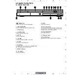
Page 133: ... dial The function is shown in the display 9 SMART JOG dial 10 STOP REC Press to stop recording 11 REC Press to start recording 12 Front panel inputs Pull the cover down where indicated to access the front panel input jacks Especially convenient for connecting camcorders and other portable equipment 13 Front panel display See Display for details 14 IR remote sensor 15 DV IN OUT jack Digital input ...

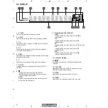
Page 134: ...has been set and during Auto Start Recording 9 Recording quality indicators FINE Lights when the recording mode is set to FINE best quality SP Lights when the recording mode is set to SP standard play LP Lights when the recording mode is set to LP long play EP Lights when the recording mode is set to EP extended play MN Lights when the recording mode is set to MN manual recording level mode 10 Cha...

Page 135: ...oneer Î mark Connect the CONTROL OUT of the other component to the CONTROL IN of this recorder using a mini plug cord 6 AC IN Power inlet 7 INPUT 3 AUTO START REC jacks Audio video inputs stereo analog audio video and S video that you can use to connect to a satellite receiver TV VCR or other source component for recording 8 OUTPUT jacks Audio video outputs stereo analog audio video and S video th...

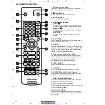
Page 136: ...buttons and CLEAR Use the number buttons for track chapter title selection channel selection and so on The same buttons can also be used to enter names for titles discs and so on Use CLEAR to clear an entry and start again 8 INPUT SELECT Press to change the input to use for recording 9 CHANNEL Press to change the channel of the built in TV tuner 10 SHOWVIEW for WYXU and WY types Press then use the...

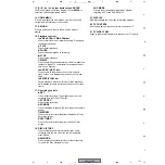
Page 137: ...t video frame 17 Recording controls REC Press to start recording Press repeatedly to set the recording time in blocks of 30 mins STOP REC Press to stop recording REC MODE Press repeatedly to change the recording mode picture quality TIMER REC Press to set a timer recording from the standard Timer Recording screen EASY TIMER Press to set a timer recording from the Easy Timer screen 18 DISC HISTORY ...

Reviews: