DVR-533H-S
114
1
2
3
4
1
2
3
4
C
D
F
A
B
E
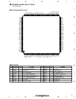
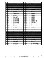
7.2 IC
PMC002A8 (JCKB ASSY : IC101)
• TUNER Microcomputer
PMC002A8, CM0041BF, R8A34011BG-K, BU4828F, R1170S331B, PQ035ZN01ZPH, NJM2861F33, BA25F18WHFP,
BD3823FV, LA73031V
No.
Pin Name
Signal Name
I/O
Function
Active
1
PA3/S08
FLDATA
O
Communication line with FL Driver
2
PA4/SI8/SB8
FLSTB
O
Ccommunication strobe line with FL Driver
3
PA5/SCK8
FLCLK
O
Communication clock with FL Driver
4
P70/INTO/TOCLP
WDT
I
WDT for detection of u-com in the state of out of control
Detection of AC power
5
P71/INT1/TOHCP
ACDET
I
6
P72/INT2/TOIN/TOLCP
HS_MTMOT
I
Handshaking of system control u-com communication
Pulse input of remote control
7
P73/INT3/TOIN/TOHCP
IR
I
8
RES#
XRESET
I
Reset input
Connection of sub clock
Connection of sub clock
Connection of main clock
Connection of main clock
9
XT1
XT1
I
10
XT2
XT2
O
11
VSS1
GND
−
12
CF1
CF1
I
13
CF2
CF2
O
14
VDD1
VDD1
−
15
P80/AN0
MODEL1
Analog In
16
P81/AN1
MODEL2
Analog In
17
P82/AN2
KEY1
Analog In
18
P83/AN3
KEY2
Analog In Main unit key input #2
Input #1 for model type judgement
Input #1 for model type judgement
Main unit key input #1
19
P84/AN4
KEY3
Analog In Main unit key input #3
AGC voltage input from tuner
Input for battery voltage checking
Detection of S tereminal #1 connection
Input for battery voltage checking
20
P85/AN5
AGC
Analog In
21
P86/AN6
BATTERY
Analog In
22
P87/AN7
FUNC
Analog In
23
P10/SO0
SDET3
I
Detection of S tereminal #3 connection
24
P11/SI0/SB0
SDET2
I
Detection of S tereminal #2 connection
25
P12/SCK0
SDET1
I
26
P13/SO1
AVLOUT
O
27
P14/SI1/SB1
SDA
Nch O/D
28
P15/SCK1
SCL
Nch O/D I2C communication (clock)
IC reset signal of whole system
Reset signal to VDEC2
29
P16/T1PWML
XSYSRST
O
I2C communication (data)
30
P17/T1PWMH/BUZ
XVDECRST
O
31
PE0/AN12
MUTEV
O
32
PE1/AN13
COMPMUTE
O
33
PE2/AN14
AMUTE1
O
34
PE3/AN15
INSEL1
O
35
PE4
INSEL2
O
Input selection of video selector
36
PE5
INSEL3
O
37
PE6
YCSEL
O
CVBS or Y/C selection of video selector
38
PE7
STBYVS
O
Standby mode selection of video selector
39
VSS4
GND
−
Input selection of video selector
40
VDD4
VDD4
−
CVBS, Y/C mute signal for video driver IC
Y/Cb/Cr mute signal for video driver IC
Audio mute signal of ouput stage
Input selection of video selector
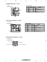
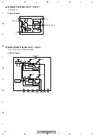
Pin Function
• The information shown in the list is basic information and may not correspond exactly to that shown in the schematic diagrams.
List of IC
Summary of Contents for DVR-531H-S
Page 17: ...DVR 533H S 17 5 6 7 8 5 6 7 8 C D F A B E ...
Page 41: ...DVR 533H S 41 5 6 7 8 5 6 7 8 C D F A B E I CN4501 To HDD CN9014 H 4 5 ...
Page 47: ...DVR 533H S 47 5 6 7 8 5 6 7 8 C D F A B E SIDE B SIDE B TUNB ASSY A A A CN101 VNP2004 A ...
Page 59: ...DVR 533H S 59 5 6 7 8 5 6 7 8 C D F A B E SIDE B SIDE B I I POWER SUPPLY UNIT I ...

