background image

2

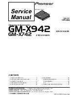
GM-X942,X742

2. EXPLODED VIEWS AND PARTS LIST

2.1 PACKING

CAUTION

This service manual is intended for qualified service technicians; it is not meant for the casual do-it-yourselfer.
Qualified technicians have the necessary test equipment and tools, and have been trained to properly and safely repair
complex products such as those covered by this manual.
Improperly performed repairs can adversely affect the safety and reliability of the product and may void the warranty.
If you are not qualified to perform the repair of this product properly and safely; you should not risk trying to do so
and refer the repair to a qualified service technician.

WARNING

This product contains lead in solder and certain electrical parts contain chemicals which are known to the state of
California to cause cancer, birth defects or other reproductive harm. 
Health & Safety Code Section 25249.6 - Proposition 65

1. SAFETY INFORMATION

-

GM-X942/X1R/UC, GM-X742/X1R/UC

Summary of Contents for GM-X742

Page 1: ...exandra Road 04 01 Singapore 159936 C PIONEER CORPORATION 2000 K ZZA JAN 2000 Printed in Japan ORDER NO CRT2454 BRIDGEABLE POWER AMPLIFIER GM X942 X1R UC EW ES Service Manual CONTENTS 1 SAFETY INFORMATION 2 2 EXPLODED VIEWS AND PARTS LIST 2 3 SCHEMATIC DIAGRAM 8 4 PCB CONNECTION DIAGRAM 20 5 ELECTRICAL PARTS LIST 28 6 ADJUSTMENT 33 7 GENERAL INFORMATION 34 7 1 DISASSEMBLY 34 7 2 IC 36 8 OPERATIONS...

Page 2: ...ormed repairs can adversely affect the safety and reliability of the product and may void the warranty If you are not qualified to perform the repair of this product properly and safely you should not risk trying to do so and refer the repair to a qualified service technician WARNING This product contains lead in solder and certain electrical parts contain chemicals which are known to the state of...

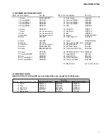
Page 3: ...6 2 CONTRAST TABLE GM X942 X1R UC EW and ES are constructed the same except for the following 1 Screw Assy HEA0049 2 Screw BYC40P180FZK 3 Polyethylene Bag HEG0011 4 Polyethylene Bag HEG0022 5 Carton See Contrast table 2 6 Contain Box See Contrast table 2 7 Protector HHP0077 8 1 Owner s Manual See Contrast table 2 8 2 Warranty Card See Contrast table 2 8 3 Owner s Manual See Contrast table 2 Mark N...

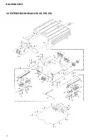
Page 4: ...4 GM X942 X742 2 2 EXTERIOR GM X942 X1R UC EW ES ...

Page 5: ...5 28 Heat Sink HNR0116 29 Bar HNR0124 30 Screw PPZ30P100SAD 31 Light Pipe Unit HXA0322 32 Screw PPZ30P100FZK 33 Thermistor TH901 902 CCX1013 34 Transistor Q908 2SB1566 35 Transistor Q907 2SD2395 36 Diode D907 FML22S 37 Diode D910 FML22R 38 FET Q905 906 911 912 STP50NE08 39 FET Q563 564 565 566 94 4980 40 FET Q567 568 569 570 94 4981 41 Transistor Q573 574 2SC1845 42 Beads Core See Contrast table 2...

Page 6: ...6 GM X942 X742 2 3 EXTERIOR GM X742 X1R UC EW ES ...

Page 7: ... Sink HNR0118 28 Bar HNR0124 29 Screw PPZ30P100SAD 30 Light Pipe Unit HXA0322 31 Screw PPZ30P100FZK 32 Thermistor TH901 902 CCX1013 33 FET Q565 566 94 4980 34 FET Q567 568 94 4981 35 Transistor Q573 574 2SC1845 36 FET Q905 906 911 912 IRFIZ44N 37 Diode D907 FML22S 38 Diode D910 FML22R 39 Transistor Q907 2SD2395 40 Transistor Q908 2SB1566 41 Beads Core See Contrast table 2 1 EXTERIOR SECTION PARTS ...

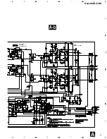
Page 8: ...en ordering service parts be sure to refer to EXPLODED VIEWS AND PARTS LIST or ELECTRICAL PARTS LIST A a A b A a A a A b A b A b A b A a A a Large size SCH diagram Guide page Detailed page A A a 20kΩ E CCS1266 20kΩ E CCS1266 ISOLATOR CIRCUIT GAIN 1 HP LP FILTER 40 120Hz 12dB OCTAVE POWER SUPPLY AMP UNIT CN851 CN851 CN852 CN852 A ...

Page 9: ...S5 C3 HZS5 C3 SML210LT LMN HEK0030 HEK0030 94 4980 94 4980 94 4980 94 4980 94 4981 94 4981 94 4981 94 4981 20kΩ C 50kΩ C 10kΩ A 10kΩ B CCP1319 10kΩ B CCP1319 BASS BOOST 40 120Hz 0 18dB OCTAVE AMP GAIN 9 7 34dB CN651 CN652 CN901 GM X942 X1R EW ES 1M ...

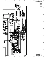
Page 10: ...10 GM X942 X742 1 2 3 4 1 2 3 4 D C B A A a A a A b 20kΩ E CCS1266 20kΩ E CCS1266 ISOLATOR CIRCUIT GAIN 1 HP LP FILTER 40 120Hz 12dB OCTAVE AMP UNIT CN851 CN851 CN852 CN852 A ...

Page 11: ...1 11 GM X942 X742 5 6 7 8 5 6 7 8 D C B A A a A a A b POWER SUPPLY 2 ...

Page 12: ...4 1 2 3 4 D C B A A a A b A b HZS5 C3 HZS5 C3 94 4980 94 4980 94 4980 94 4980 94 4981 94 4981 94 4981 94 4981 20kΩ C 50kΩ C 10kΩ A 10kΩ B CCP1319 10kΩ B CCP1319 BASS BOOST 40 120Hz 0 18dB OCTAVE AMP GAIN 9 7 34dB CN651 CN652 ...

Page 13: ...1 13 GM X942 X742 5 6 7 8 5 6 7 8 D C B A A b A a A b SML210LT LMN HEK0030 HEK0030 94 4981 94 4981 CN901 GM X942 X1R EW ES 1M 2 ...

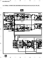
Page 14: ...4 D C B A 3 2 OVERALL CONNECTION DIAGRAM GUIDE PAGE GM X742 X1R UC EW ES A A a 100 16 100 16 20KΩ E 20KΩ E 20KΩ C 50KΩ C ISOLATOR CIRCUIT GAIN 1 AMP UNIT A HP LP FILTER 40 120Hz 12dB OCTAVE B 4 0 POWER SUPPLY CN851 CN852 CN852 CN851 ...

Page 15: ...A 100 16 100 16 470 16 HZS5 C3 HZS5 C3 SML210LT LMN HEK0020 20A HEK0020 20A 2SC2458 94 4980 94 4980 94 4981 94 4981 R697 10KΩ A CCP1319 10KΩ B CCP1319 10KΩ B BASS BOOST 40 120Hz 0 18dB OCTAVE AMP GAIN 8 8 33dB CN901 CN652 CN651 GM X742 X1R EW ES ...

Page 16: ...16 GM X942 X742 1 2 3 4 1 2 3 4 D C B A A a A a A b 20KΩ E 20KΩ E 20KΩ C 50KΩ C ISOLATOR CIRCUIT GAIN 1 AMP UNIT A HP LP FILTER 40 120Hz 12dB OCTAVE BA 40 0 CN851 CN852 CN852 CN851 ...

Page 17: ...1 17 GM X942 X742 5 6 7 8 5 6 7 8 D C B A A a A a A b 100 16 100 16 POWER SUPPLY 2 ...

Page 18: ... X742 1 2 3 4 1 2 3 4 D C B A A a A b A b 100 16 100 16 HZS5 C3 HZS5 C3 2SC2458 94 4980 94 4980 94 4981 94 4981 10KΩ A CCP1319 10KΩ B CCP1319 10KΩ B BASS BOOST 40 120Hz 0 18dB OCTAVE AMP GAIN 8 8 33dB CN652 CN651 ...

Page 19: ...1 19 GM X942 X742 5 6 7 8 5 6 7 8 D C B A A b A a A b 470 16 SML210LT LMN HEK0020 20A HEK0020 20A R697 CN901 GM X742 X1R EW ES 2 ...

Page 20: ...rts mounted on this PCB include all necessary parts for several destination For further information for respective destinations be sure to check with the schematic dia gram 2 Viewpoint of PCB diagrams A Capacitor Connector P C Board Chip Part SIDE A SIDE B 1 2 3 1 2 3 1 2 3 1 2 3 3 2 1 3 2 1 3 2 1 3 2 1 L R L PRE OUT R A AMP UNIT ...

Page 21: ...21 GM X942 X742 5 6 7 8 5 6 7 8 D C B A A SIDE A 1 2 3 1 2 3 1 2 3 1 2 3 1 2 3 3 2 1 R B REMOTE B GND R L L ...

Page 22: ...22 GM X942 X742 1 2 3 4 1 2 3 4 D C B A A A AMP UNIT ...

Page 23: ...23 GM X942 X742 5 6 7 8 5 6 7 8 D C B A A SIDE B ...

Page 24: ...24 GM X942 X742 1 2 3 4 1 2 3 4 D C B A 4 2 AMP UNIT GM X742 X1R UC EW ES A L R L PRE OUT R 3 2 1 3 2 1 A AMP UNIT ...

Page 25: ...25 GM X942 X742 5 6 7 8 5 6 7 8 D C B A A SIDE A 3 2 1 3 2 1 1 2 3 1 2 3 1 2 3 1 2 3 R B REMOTE B GND R L L ...

Page 26: ...26 GM X942 X742 1 2 3 4 1 2 3 4 D C B A A A AMP UNIT ...

Page 27: ...27 GM X942 X742 5 6 7 8 5 6 7 8 D C B A A SIDE B ...

Page 28: ... 2SC2458 Q 659 Transistor 2SA1048 Q 660 Transistor 2SB1243 Q 661 Transistor 2SC2458 Q 902 Transistor 2SA1048 Q 903 Transistor 2SB1277 Q 904 Transistor 2SB1277 Q 905 FET STP50NE08 Q 906 FET STP50NE08 Q 907 Transistor 2SD2395 Q 908 Transistor 2SB1566 Q 909 Transistor 2SD1919 Q 910 Transistor 2SD1919 Q 911 FET STP50NE08 Q 912 FET STP50NE08 D 501 Diode HZS5 C3 D 502 Diode HZS5 C3 D 551 Diode 1SS133 D ...

Page 29: ...88 SPR30R1J R 589 SPR30R1J R 590 SPR30R1J R 591 SPR30R1J R 592 SPR30R1J R 593 SPR30R1J R 594 SPR30R1J R 597 RD1 4PU564J R 598 RD1 4PU564J R 599 RD1 4PU473J R 600 RD1 4PU473J R 601 RS1 2PMF100J R 602 RS1 2PMF100J R 605 RD1 4PU331J R 606 RD1 4PU331J R 657 RD1 4PU104J R 658 RD1 4PU472J R 659 RD1 4PU103J R 660 RD1 4PU102J R 661 RD1 4PU472J R 662 RD1 4PU221J R 663 RD1 4PU563J R 664 RD1 4PU473J R 665 RD...

Page 30: ...A103J50 C 558 CFTLA103J50 C 559 CCPUCH150J50 C 560 CCPUCH150J50 C 561 337RZM050M1020 C 562 337RZM050M1020 C 563 337RZM050M1020 C 564 337RZM050M1020 C 567 CFTNA333J50 C 568 CFTNA333J50 C 569 CQMA102J50 C 570 CQMA102J50 C 571 CMA330J2H C 572 CMA330J2H C 651 220µF 10V CCH1036 C 652 CFTLA103J50 C 653 CEAS100M16 C 654 CEAS100M16 C 655 CFTLA103J50 C 656 470µF 16V CCH1183 C 658 CEAS220M16 C 659 470µF 16V...

Page 31: ...ML210LT LMN D 653 Diode 1SS133 D 654 Diode HZS7L B2 D 658 Diode 1SS133 D 659 Diode 1SS133 D 661 Diode 1SS133 D 701 Diode ERA15 02VH D 702 Diode ERA15 02VH D 903 Diode RM4Z D 907 Diode FML22S D 908 Diode HZS16L 1 D 909 Diode HZS16L 1 D 910 Diode FML22R L 801 Ferri Inductor CTF1007 L 802 Ferri Inductor CTF1007 T 901 Transformer HTT0007 TH 901 Thermistor CCX1013 TH 902 Thermistor CCX1013 TH 903 Therm...

Page 32: ...R 680 RS1 10S472J R 681 RD1 4PU821J R 682 RD1 4PU821J R 683 RD1 4PU103J R 684 RD1 4PU223J R 685 RD1 4PU223J R 686 RD1 4PU223J R 697 RD1 4PU0R0J R 851 RS1 10S471J R 852 RS1 10S471J R 853 RS1 10S223J R 854 RS1 10S223J R 855 RN1 10SE1002D R 856 RN1 10SE1002D R 857 RN1 10SE1002D R 858 RN1 10SE1002D R 859 RN1 10SE1002D R 860 RN1 10SE1002D R 861 RN1 10SE1002D R 862 RN1 10SE1002D R 865 RS1 10S821J R 866 ...

Page 33: ...9 470µF 16V CCH1183 C 661 CFTLA103J50 C 662 CFTLA103J50 C 663 CFTLA334J50 C 664 CKSQYB223K50 C 851 CKSQYB471K50 C 852 CKSQYB471K50 C 853 CEAS100M16 C 854 CEAS100M16 C 855 CFTNA104J50 C 856 CFTNA104J50 C 857 CCSQCH470J50 C 858 CCSQCH470J50 C 859 CCSQCH470J50 C 860 CCSQCH470J50 C 861 CKSQYB471K50 C 862 CKSQYB471K50 C 863 CEAS4R7M35 C 864 CEAS4R7M35 C 865 CCSQCH470J50 C 867 CCSSL101J50 C 868 CCSSL101...

Page 34: ...emoving the Case Fig 1 Remove the six screws Remove the three screws Remove the four screws and then remove the Case Removing the Amp Unit Remove the screw and then remove the Plate Fig 1 Remove the two screws Fig 2 Remove the ten screws and then remove the Amp Unit Not shown Fig 2 Plate ...

Page 35: ...e screw and then remove the Plate Fig 3 Remove the two screws Fig 4 Remove the ten screws and then remove the Amp Unit Not shown Case Fig 3 Removing the Case Fig 3 Remove the four screws Remove the three screws Remove the four screws and then remove the Case Plate Fig 4 ...

Page 36: ... 14 15 16 VCC Stby DET1 DET2 DET_R GND NC NC IN1 IN2 IN3 Cont_V Filter Vs_out TC Mute_out zz 2V zz 2V zz 2V 2V zz 2V 20µA zz 2V zz 50µA 4 7kΩ Transient voltage detector Bandgap Circuit motion on 5 6V Q S R Oneshot 1µsec Bandgap on Switch on 0 13V PA2027A ...

Page 37: ...37 GM X942 X742 8 OPERATIONS AND SPECIFICATIONS 8 1 OPERATIONS ...

Page 38: ...st frequency control from 0 to 18 dB Cut Off Frequency Control If the LPF HPF select switch is set to LPF or HPF you can select a cut off frequency from 40 to 120 Hz Bass Boost Frequency Control You can select a bass boost frequency from 40 to 120 Hz with the bass boost control Bass Boost Level Control and Bass Boost Frequency Control can be adjusted only when the LPF HPF select switch is set to a...

Page 39: ...X742 Fuse 20 A 2 Car stereo with RCA output jacks External Output Connecting wires with RCA pin plugs sold separately RCA input jack RCA output jack Speaker output terminal System remote control wire sold separately Connect the male terminal of this wire to the system remote control terminal of the car stereo SYSTEM REMOTE CONTROL The female terminal can be connected to the auto antenna relay cont...

Page 40: ...0 8 THD Load impedance 4 Ω 1 8 Ω allowable Bridge connection 2 8 Ω allowable Frequency response 10 50 000 Hz 0 dB 1 dB Signal to noise ratio 105 dB IHF A network Distortion 0 005 10 W 1 kHz Separation 65 dB 1 kHz Low pass filter Cut off frequency 40 120 Hz Cut off slope 12 dB oct High pass filter Cut off frequency 40 120 Hz Cut off slope 12 dB oct Bass boost Frequency 40 120 Hz Gain 0 18 dB Maximu...

Page 41: ...e Frequency response 10 50 000 Hz 0 dB 1 dB Signal to noise ratio 105 dB IEC A network Distortion 0 005 10 W 1 kHz Separation 65 dB 1 kHz Low pass filter Cut off frequency 40 120 Hz Cut off slope 12 dB oct High pass filter Cut off frequency 40 120 Hz Cut off slope 12 dB oct Bass boost Frequency 40 120 Hz Gain 0 18 dB Maximum input level impedance 6 5 V 22 kΩ 0 4 6 5 V Note Specifications and the d...

Page 42: ...1 8 Ω allowable Bridge connection 2 8 Ω allowable Frequency response 10 50 000 Hz 0 dB 1 dB Signal to noise ratio 105 dB IEC A network Distortion 0 005 10 W 1 kHz Separation 65 dB 1 kHz Low pass filter Cut off frequency 40 120 Hz Cut off slope 12 dB oct High pass filter Cut off frequency 40 120 Hz Cut off slope 12 dB oct Bass boost Frequency 40 120 Hz Gain 0 18 dB Maximum input level impedance 6 5...

Page 43: ...ad impedance 4 Ω 1 8 Ω allowable Bridge connection 2 8 Ω allowable Frequency response 10 50 000 Hz 0 dB 1 dB Signal to noise ratio 105 dB IHF A network Distortion 0 005 10 W 1 kHz Separation 65 dB 1 kHz Low pass filter Cut off frequency 40 120 Hz Cut off slope 12 dB oct High pass filter Cut off frequency 40 120 Hz Cut off slope 12 dB oct Bass boost Frequency 40 120 Hz Gain 0 18 dB Maximum input le...

Page 44: ...e Frequency response 10 50 000 Hz 0 dB 1 dB Signal to noise ratio 105 dB IEC A network Distortion 0 005 10 W 1 kHz Separation 65 dB 1 kHz Low pass filter Cut off frequency 40 120 Hz Cut off slope 12 dB oct High pass filter Cut off frequency 40 120 Hz Cut off slope 12 dB oct Bass boost Frequency 40 120 Hz Gain 0 18 dB Maximum input level impedance 6 5 V 22 kΩ 0 4 6 5 V Note Specifications and the d...

Page 45: ... 8 Ω allowable Bridge connection 2 8 Ω allowable Frequency response 10 50 000 Hz 0 dB 1 dB Signal to noise ratio 100 dB IEC A network Distortion 0 005 10 W 1 kHz Separation 60 dB 1 kHz Low pass filter Cut off frequency 40 120 Hz Cut off slope 12 dB oct High pass filter Cut off frequency 40 120 Hz Cut off slope 12 dB oct Bass boost Frequency 40 120 Hz Gain 0 18 dB Maximum input level impedance 6 5 ...

Reviews: