17
HTP-071
5
6
7
8
5
6
7
8
A
B
C
D
E
F
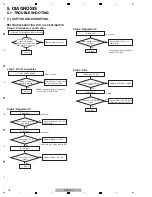
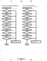
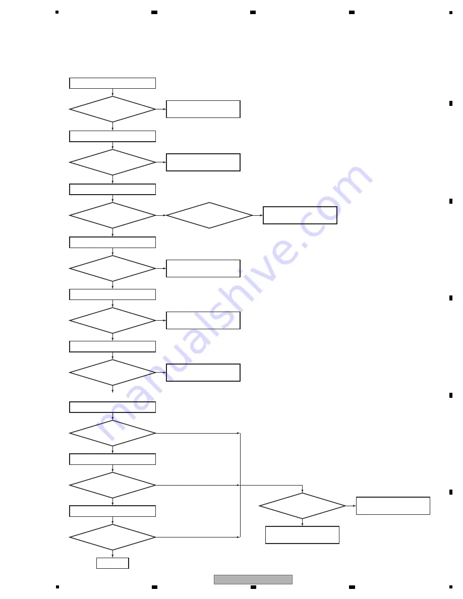
Check the path to OUTPUT
pin of JACK601, JACK602.
Check the path to pins 4, 8
of IC600 or replace IC600.
Yes
Step 5: DIR
IC600 (pins 3,11)
IC602 (pins 31, 37)
IC602 (pin 20)
IC602 (pin 18)
IC602 (pin 17)
Can observe the
digital signal?
Check that the S/PDIF signal is output.
Check that changes by pulling out and inserting the digital input lines.
N
o
Yes
Can observe the
digital signal?
Is there a master
clock output?
Is the voltage of PD
N
IC602 pin 34 3.3 V?
Yes
N
o
N
o
31: OPTICAL
37: COXIAL
DIR_SCKO (master clock)
DIR_LRCK (LR CLOCK)
DIR_SDTO (DATA)
DIR_BCK (bit clock)
3: OPTICAL
11: COXIAL
(0 V
↔
3.3 V)
(0 V
↔
3.3 V)
Replace IC602.
Yes
Is there a LR clock
output?
IC602 (pin 19)
Yes
N
o
Check the MAI
N
Assy.
N
o
(0 V
↔
3.3 V)
Replace IC602.
Is there a DATA
output?
N
o
(0 V
↔
3.3 V)
Yes
Replace IC602.
Replace IC101.
Is there a bit clock
output?
N
o
Check the path between
IC101 pin 1 and MAI
N
Assy.
N
o
(0 V
↔
3.3 V)
SWITCH
DAI_MCK (MASTER CLOCK)
IC101 (pin 4)
Yes
Is there a master clock
output?
N
o
(0 V
↔
2.5 V)
DAI_LRCK (LR CLOCK)
*IC101 pin 1
0 V: DIR
3.3 V: HDMI
DAI_bck (bit CLOCK)
IC101 (pin 7)
IC101 (pin 9)
Yes
Yes
Is there a LR clock
output?
N
o
(0 V
↔
2.5 V)
Yes
Is there a bit clock
output?
Is the voltage of
IC101 pin 1 0V?
N
o
(0 V
↔
2.5 V)
To Step 6
Summary of Contents for HTP-071
Page 9: ...9 HTP 071 5 6 7 8 5 6 7 8 A B C D E F ...
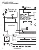
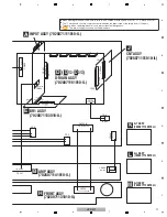
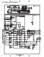
Page 12: ...12 HTP 071 1 2 3 4 A B C D E F 1 2 3 4 4 2 OVERALL BLOCK DIAGRAM H FRONT ASSY A INPUT ASSY ...
Page 89: ...89 HTP 071 5 6 7 8 5 6 7 8 A B C D E F C SIDE B CP1 CP3 CP5 CN1 CN3 ...
Page 93: ...93 HTP 071 5 6 7 8 5 6 7 8 A B C D E F D SIDE B CN600 CP104 ...

