1
8
HTP-071
1
2
3
4
A
B
C
D
E
F
1
2
3
4
Yes
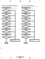
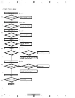
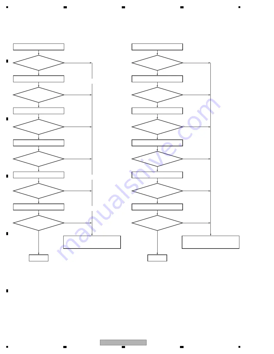
Step 6: DSP output (digital) to CODEC input
IC601 (pin 7)
IC601 (pin8 )
Is there a bit clock
input?
Digital output of each CH when inputting the digital signal with audio.
Is there a LR clock
output?
Is there a data input?
Is there a data input?
Is there a data input?
Is there a data input?
Yes
IC601 (pin 6)
IC601 (pin11)
Yes
IC601 (pin 11)
Yes
IC601 (pin 13)
Yes
Yes
DSP_BCK (BIT CLOCK)
front L/R data
surround L/R data
(0 V
↔
3.3 V)
(0 V
↔
3.3 V)
(0 V
↔
3.3 V)
(0 V
↔
3.3 V)
(0 V
↔
3.3 V)
(0 V
↔
3.3 V)
To Step 7
N
o
N
o
N
o
N
o
N
o
N
o
Check the path between IC102
and data & address lines.
SDRAM (IC103), FLASH ROM (IC104).
Replace IC602, IC603, IC604,
IC605 and IC606.
Yes
Step 7: CODEC output (ANALOG)
IC603 (pin 1)
IC603 (pin 7 )
Is there a audio signal
output?
Analog output of each CH when inputting the digital signal with audio.
Yes
Is there a audio signal
output?
front R out
front L out
IC604 (pin 1)
Yes
Is there a audio signal
output?
surround R out
IC604 (pin7)
Yes
Is there a audio signal
output?
surround L out
IC605 (pin1)
Yes
Is there a audio signal
output?
center out
IC605 (pin7)
Yes
Is there a audio signal
output?
LFE out
End
N
o
N
o
N
o
N
o
N
o
N
o
DSP_LRCK (LR CLOCK)
CE
N
TER/LFE data
surround back L/R data
Summary of Contents for HTP-071
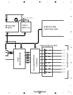
Page 9: ...9 HTP 071 5 6 7 8 5 6 7 8 A B C D E F ...
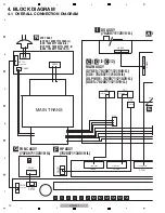
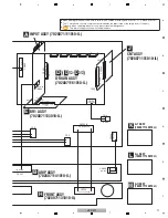
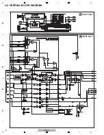
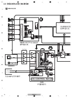
Page 12: ...12 HTP 071 1 2 3 4 A B C D E F 1 2 3 4 4 2 OVERALL BLOCK DIAGRAM H FRONT ASSY A INPUT ASSY ...
Page 89: ...89 HTP 071 5 6 7 8 5 6 7 8 A B C D E F C SIDE B CP1 CP3 CP5 CN1 CN3 ...
Page 93: ...93 HTP 071 5 6 7 8 5 6 7 8 A B C D E F D SIDE B CN600 CP104 ...

