HTZ-7, HTZ-C7, HTZ-SW7, HTZ-ST7
101
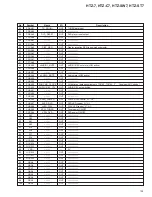
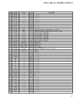
No. Name I/O
Description
14
Vss
––
GND terminal
15
DO1
O
Digital data output terminal 1
16
DO2
O
Digital data output terminal 2
17
M1
I
Channel mode setting terminal 1
18
M2
I
Channel mode setting terminal 2
19
IS1
I
Data input mode setting terminal 1
20
IS2
I
Data input mode setting terminal 2
21
CTG1
I
Parallel setting mode: Category code setting terminal 1
Serial setting mode: Data input terminal
22
CTG2
I
Parallel setting mode: Category code setting terminal 2
Serial setting mode: Clock input terminal
23
CTG3
I
Parallel setting mode: Category code setting terminal 3
Serial setting mode: Latch pulse input terminal
24
FR32
O
FR32 output terminal
25
LBIT
I
Parallel setting mode: LBIT input terminal 1
Serial setting mode: 32/192 bit switching terminal
26
CKA1
I
Parallel setting mode: Clock accuracy setting terminal 1
Serial setting mode: Fixed to “H”
27
CKA2
I
Parallel setting mode: Clock accuracy setting terminal 2
Serial setting mode: Output prohibited, fixed to “H”
28
VDD
––
Power supply voltage terminal
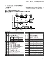
7. GENERAL INFORMATION
7.1 PARTS
7.1.1 IC
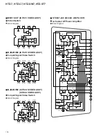
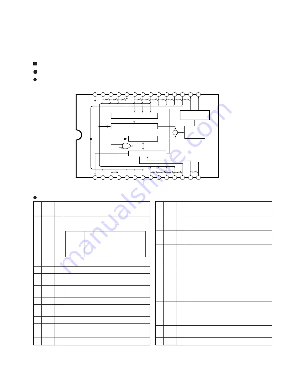
Digital Audio Interface Modulation and Transmission IC
Block Diagram
TC9271F (IC7008: SVIDEO ASSY)
No. Name I/O
Description
1 BLOCK O
Block leading head position detection terminal
2
UBDA
I
User bit data input terminal
3
LRS
I
LRCK polarity selection terminal
4
LRCK
I
LR clock input terminal
5
BCK
I
Bit clock input terminal
6
DATA
I
2-channel mode: Data input terminal
4-channel mode: Data input terminal 1
7
VLDY
I
2-channel mode: Compensation flag input terminal
4-channel mode: Data input terminal 2
8
EMPH
I
Emphasis flag setting terminal
9
COPY
I
Parallel setting mode: Copy flag setting terminal
Serial setting mode: Fixed to “H”
10
FS1
I
Sampling frequency setting terminal 1
11
FS2
I
Sampling frequency setting terminal 2
12
CKS
I
Clock division selection terminal
13
XI
I
Clock input terminal
LRS
LRCK
L
R
L Level
R ch Data
L ch Data
L Level
L ch Data
R ch Data
Pin Function
CTG3
CTG2
CTG1
EMPH
COPY
FS1
23
22
21
10
FS2
11
CKA2
CKA1
LBIT
27
26
25
8
9
LRS
LRCK
BCK
DATA
VLDY
3
4
7
UBDA
2
5
6
IS2
IS1
M2
M1
20
19
18
17
DO2
DO1
16
15
CKS
XI
BLOCK
12
13
1
FR32
24
Vss
14
VDD
28
+
Serial Interface
Biphase Mark
Modulation Circuit
Parity
Generation
Circuit
Data Input Circuit
Category Code Register
Clock Generation Circuit
The information shown in the list is basic information and may not
correspond exactly to that shown in the schematic diagrams.


