background image

PD-F607, PD-F507

2

1. SAFETY INFORMATION

Additional Laser Caution

1. Laser Interlock Mechanism

The position of the switch (S651) for detecting loading
state is detected by the system microprocessor, and
the design prevents laser diode oscillation when the
switch (S651) is not on CLMP terminal side (CLMP
signal is OFF or high level).
Thus, the interlock will no longer function if the switch (S651)
is deliberatery set to CLMP terminal side. (low level)
The  interlock also does not function in the test mode 

.

Laser diode oscillation will continue, if pin 33 of
CXA1782CQ (IC151) on the MOTHER BOARD ASSY
is connected to GND, or pin 26 of IC351 (LDON) is
connected to low level (ON), or else the terminals of
Q151 are shorted to each other (fault condition).

2. When the cover is opened, close viewing of the

objective lens with the naked eye will cause exposure
to a Class 1 laser beam.

 : Refer to page 25. on the service manual RRV1877.

This  service  manual  is  intended  for qualified  service  technicians;  it  is  not  meant  for  the  casual
do-it-yourselfer. Qualified technicians have the necessary test equipment and tools, and have been
trained to properly and safely repair complex products such as those covered by this manual.
Improperly performed repairs can adversely affect the safety and reliability of the product and may
void the warranty. If you are not qualified to perform the repair of this product properly and safely, you
should not risk trying to do so and refer the repair to a qualified service technician.

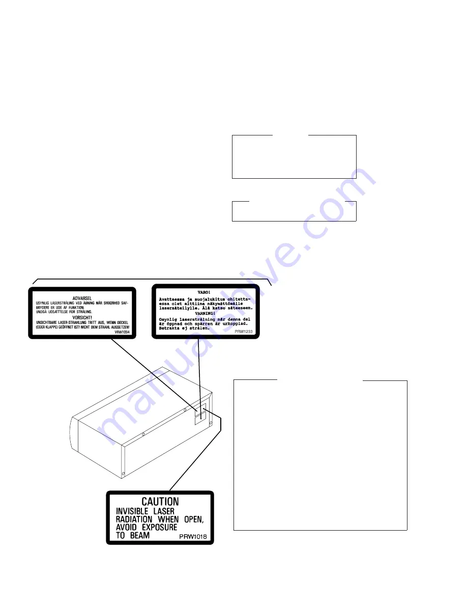
LABEL CHECK (For PD-F607/WYXJ,WVXJ and PD-F507/WPWXJ only)

REAR

PD-F607/WVXJ and  PD-F507/WPWXJ only

PD-F607/WYXJ only


                          IMPORTANT

THIS   PIONNER   APPARATUS   CONTAINS
LASER   OF   CLASS  1.
SERVICING OPERATION OF THE APPARATUS
SHOULD   BE   DONE   BY   A   SPECIALLY
INSTRUCTED  PERSON.


LASER DIODE CHARACTERISTICS

MAXIMUM OUTPUT POWER : 5 mw
WAVELENGTH : 780-785 nm

Summary of Contents for PD-F507

Page 1: ...8 FILE TYPE CD PLAYER RRV1951 PD F607 T ZZY APR 1998 Printed in Japan Refer to the service manual RRV1877 for PD F607 KUXJ and PD F507 KUXJ CONTENTS 1 SAFETY INFORMATION 2 2 CONTRAST OF MISCELLANEOUS PARTS 3 3 SCHEMATIC AND PCB DIAGRAMS 8 THIS MANUAL IS APPLICABLE TO THE FOLLOWING MODEL S AND TYPE S Model PD F607 PD F507 Type The voltage can be converted by the following method Power Requirement W...

Page 2: ...eye will cause exposure to a Class 1 laser beam Refer to page 25 on the service manual RRV1877 This service manual is intended for qualified service technicians it is not meant for the casual do it yourselfer Qualified technicians have the necessary test equipment and tools and have been trained to properly and safely repair complex products such as those covered by this manual Improperly performe...

Page 3: ...G P3 1 Operating Instructions English PRB1262 Not used PRB1265 P3 1 Operating Instructions Not used PRE1265 Not used English French P3 1 Operating Instructions Not used PRD1026 Not used German Italian Dutch Swedish Spanish Portuguese P3 5 Control Cable L 1m PDE1247 Not used Not used P3 10 Packing Case PHG2282 PHG2298 PHG2299 P3 12 NSP Warranty Card ARY1051 ARY7009 ARY7009 CD Liner Notes File Not u...

Page 4: ... No 1 Index Label Sheet 25 Not used PRW1422 PRW1422 PRW1422 PRW1422 No 2 Caution 220V Label Not used Not used Not used ARR1003 ARR1003 No 13 EXTERIOR P5 2 Cord Stopper CM 22C CM 22B CM 22B CM 22B CM 22B P5 4 AC Power Cord PDG1015 ADG1123 PDG1062 PDG1003 PDG1056 P5 5 Power Transformer AC120V PTT1237 Not used Not used Not used Not used P5 5 Power Transformer AC220 240V Not used PTT1236 PTT1236 Not u...

Page 5: ...Case No 2 No 1 Front Polyetylene Bag No 3 Protecter F Protecter F Protecter R Protecter R Operating Instructions Warranty Card Remote Control unit Batteery Control Cable N0 13 Rear Base Under Base Foot Screw BBZ30P060FMC Screw IBZ30P080FMC No 12 Control Panel No 5 No 6 No 8 No 7 No 11 No 10 No 9 ...

Page 6: ...AT101M10 C311 C314 C316 C322 C352 CEAT101M10 C52 CEAT101M35 C26 CEAT102M16 C433 C434 CEAT220M25 C131 C133 C27 CEAT330M16 C25 CEAT332M16 C351 CEAT471M6R3 C169 C170 C356 CEAT4R7M50 C309 CEATR47M50 C156 C161 C164 C168 C218 CGCYX103K25 C321 CGCYX104K25 C160 CGCYX333K25 C167 CGCYX472K25 C152 C307 CGCYX473K25 C163 CKCYB102K50 C176 C306 C441 C442 CKCYB152K50 C305 CKCYB222K50 C162 CKCYB332K50 C151 CKCYB68...

Page 7: ...151 CKCYB682K50 C11 C13 C15 CKCYF103Z50 C159 CKCYF103Z50 C16 C17 CKCYF103Z50 C172 C173 C205 C210 C215 CKCYF103Z50 C219 C29 C304 C310 CKCYF103Z50 C312 C313 C317 C319 CKCYF103Z50 C323 C325 C353 C354 C357 CKCYF103Z50 C387 C405 C417 C461 C471 CKCYF103Z50 C153 C155 C158 C382 CQMA104J50 C157 CQMA823J50 RESISTORS VR153 VR155 10kΩ RCP1045 VR151 VR152 VR154 22kΩ RCP1046 VR156 220kΩ RCP1049 Other Resistors ...

Page 8: ... RLXJ RDXJ PWM2195 SIGNAL ROUTE AUDIO SIGNAL FOCUS SERVO LOOP TRACKING SERVO LOOP CARRIAGE SERVO LOOP SPINDLE DRIVE LOADING DRIVE 23 16 19 18 53 33 2 23 4 3 7 5 6 8 5 0V 1 7V 1 7V 0 2V 1 6V 1 6V 0V 1 6V 1 6V 0V 1 8V 1 8V 0 7V CN701 J801 CN653 STBL PD F607 OTHERS R351 220 150 D352 Jumper 1SS254 R310 R311 R312 DATA LRC BCK1 PD F607 OTHERS R310 R312 220 Jumper PD F507 Only PD F607 Only PD F607 Only C...

Page 9: ...123 PD F507 MAMXJ PDG1062 PD F507 RDXJ PDG1056 Power Requirement WYXJ WVXJ WPWXJ AC220 240 50 60Hz RLXJ AC110 120V 220 240V 50 60Hz RDXJ AC110 127V 220 240V 50 60Hz MAMXJ AC220 230V 50 60Hz WYXJ WVXJ PTT1236 WPWXJ MAMXJ PTT1236 RLXJ RDXJ PTT1238 RDXJ RLXJ OTHER JP1 JP2 S5 HEADPHONE ASSY PWX1549 PD F607 Only PD F607 Only EXCEPT PD F607 R360 R361 PD F607 OTHER EXCEPT PD F507 WPWXJ PD F607 OTHERS D32...

Page 10: ...he parts mounted on this PCB include all necessary parts for several destination For further information for respective destinations be sure to check with the schematic diagram 4 Viewpoint of PCB diagrams Symbol in PCB Diagrams Symbol in Schematic Diagrams Part Name Transistor Transistor with resistor Field effect transistor B C E B C E B C E D G S B C E B C E B C E D G S D G S Resistor array 3 te...

Reviews: