PDP-425CMX
179
5
6
7
8
5
6
7
8
C
D
F
A
B
E
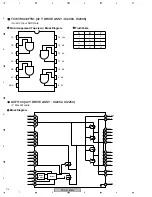
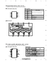
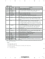
Pin Name
I/O
No.
Description
AnP
I
*A
Positive LVDS differential data inputs.
AnM
I
*B
Negative LVDS differential data inputs.
Rn,Gn,Bn,
DE,HSYNC,
VSYNC
O
*C
69/71/70
TTL level data outputs. This includes: 16 Red, 16 Green, 16 Blue, and 3
control lines – HSYNC (LP), VSYNC (FLM), DE (Data Enable).
RxCLK INP
I
91
Positive LVDS differential clock input.
RxCLK INM
I
92
Negative LVDS differential clock input.
RxCLK OUT
O
42
TTL level clock output. The falling edge acts as data strobe.
R_FDE
I
77
Programmable control (DE) strobe select. Tied high for data active when DE
is high.
PLLSEL
I
5
PLL range select. This pin must be tied to V
CC
for auto-range. NC or tied to
Ground is reserved for future use. Typical shift point is between 55 and 68
MHz.
BAL
I
6
Mode select for DC Balanced (new) or non-DC Balanced (backward
compatible) interface. BAL = LOW fornon-DC Balanced mode. BAL = HIGH
for DC Balanced Mode (Auto-detect mode), with this pin HIGH the received
LVDS clock signal is used to determine if the interface is in new or backward
compatible mode (Notes 1) .
DESKEW
I
4
Deskew and oversampling “on/off“ select. Deskew is active when in put is
high. Only supported in DC Balance mode (BAL = High). To complete the
deskew operation, a minimum of four clock cycles is required during
blanking time.
PD
I
78
TTL level in put. When asserted (low input) the receiver data outputs are low
and clock out put is high.
STOPCLK
O
73
Indicates receiver clock in put signal is not present with a logic high. With a
clock input present, alow logic is indicated.
V
CC
I
*D
Power supply pins for TTL outputs and digital circuitry.
GND
I
*E
*D : 13, 23, 33, 45, 56, 66
*C : 8–12, 14, 15, 17–22, 24, 26–32, 34, 36–41, 43, 46–53, 55, 57–62, 64, 65, 67, 68
*E : 7, 16, 25, 35, 44, 54, 63, 72
*A : 79, 82, 84, 86, 89, 94, 96, 98
*B : 80, 83, 85, 87, 90, 95, 97, 99
Ground pins for TTL outputs and digital circuitry
PLLV
CC
I
2
Power supply for PLL circuitry.
PLLGND
I
1, 3
Ground pin for PLL circuitry.
LVDSV
CC
I
81, 93
Power supply pin for LVDS inputs.
LVDSGND
I
76, 88, 100
Ground pins for LVDS in puts.
CNTLE,
CNTLF
O
75
74
TTL level data outputs. User-defined control signals - no connect when not
used.
Note 1 :
The DS90CF388 is designed to automatically detect the DC Balance or non-DC Balance transmitted data from the DS90C387 and deserialize the LVDS
data according to the defined bit mapping.
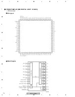
Pin Function
[Pin No.]
Summary of Contents for PDP-42MXE10
Page 9: ...PDP 425CMX 9 5 6 7 8 5 6 7 8 C D F A B E ...
Page 27: ...PDP 425CMX 27 5 6 7 8 5 6 7 8 C D F A B E ...
Page 37: ...PDP 425CMX 37 5 6 7 8 5 6 7 8 C D F A B E ...
Page 129: ...PDP 425CMX 129 5 6 7 8 5 6 7 8 C D F A B E ...
Page 132: ...PDP 425CMX 132 1 2 3 4 1 2 3 4 C D F A B E MAIN PWB CONNECTOR WAVE FORM POINT SIDE B ...


