PDP-425CMX
41
5
6
7
8
5
6
7
8
C
D
F
A
B
E
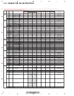
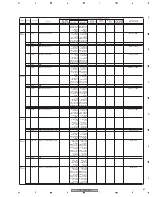
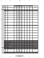
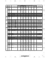
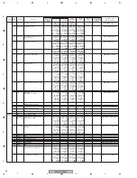
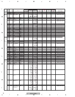
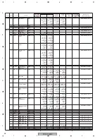
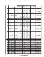
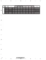
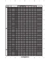
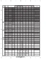
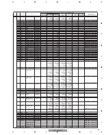
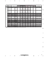
Name
MAIN POWER "ON"
Basic operation(Numerical unit:Vdc; except for case when units are individually indicated)
No signal
With signal
"Signal direction
(DR : Data Relay)"
"AC power ON
(Power cord
connected to the
wall outlet) "
"AC Power OFF
(Power cord pulled
out of the wall outlet
"
"Power
management
"
Standby
"Main power
OFF
"
Pin name
Pin No.
TM2
CN1001
TM3
CN1201
TM4
CN1101
FA
CN9003
FB
CN9004
4
1
2
3
4
5
6
7
8
1
2
3
4
5
6
7
8
1
2
3
4
1
2
3
1
2
SDA5
SCL5
GND
VDD+3.3V
SDA5
SCL5
GND
VDD+3.3V
SDA5
SCL5
GND
VDD+3.3V
SDA5
SCL5
GND
VDD+3.3V
SDA5
SCL5
GND
VDD+3.3V
SDA5
FAN-CTL
GND
F_ALM
FAN-CTL
GND
Data line of the I2C bus
Clock line of the I2C bus
GND
3.3V power supply for analog signals
Data line of the I2C bus
Clock line of the I2C bus
GND
3.3V power supply for analog signals
Data line of the I2C bus
Clock line of the I2C bus
GND
3.3V power supply for analog signals
Data line of the I2C bus
Clock line of the I2C bus
GND
3.3V power supply for analog signals
Data line of the I2C bus
Clock line of the I2C bus
GND
3.3V power supply for analog signals
Data line of the I2C bus
Voltage- controllable power supply
GND
Fan lock detect signal output
Voltage- controllable power supply
GND
0
0
0
0
0
0
0
0
0
0
0
0
0
0
0
0
0
0
0
0
0
0
0
0
0
0
During data
exchange: Clock
signal (3.3Vac),
datanot
exchanged:
3.3Vdc
Clock signal
used during
data
transmission
(3.3Vac), 3.3Vdc
when no data
are transmitted
0
3.3
During data
exchange:
Clock signal
(3.3Vac),datanot
exchanged:
3.3Vdc
Clock signal
used
during data
transmission
(3.3Vac), 3.3Vdc
when no data
are transmitted
0
3.3
During data
exchange:
Clock signal
(3.3Vac),datanot
exchanged:
3.3Vdc
Clock signal
used
during data
transmission
(3.3Vac), 3.3Vdc
when no data
are transmitted
0
3.3
During data
exchange:
Clock signal
(3.3Vac),datanot
exchanged:
3.3Vdc
Clock signal
used
during data
transmission
(3.3Vac), 3.3Vdc
when no data
are transmitted
0
3.3
During data
exchange:
Clock signal
(3.3Vac),datanot
exchanged:
3.3Vdc
Clock signal
used during
data
transmission
(3.3Vac),
3.3Vdc when
no data
are transmitted
0
3.3
During data
exchange:
Clock signal
(3.3Vac),datanot
exchanged:
3.3Vdc
11.6Vdc during
high-speed
revolition
(Fan mode H) ;
8.8Vdc during
medium speed
revolition
(Fan mode M) ;
6.0Vdc during
low-speed
revolition
(Fan mode L) ;
0
0V during
normal Fan
operation;
3.3Vdc while
the fan is
stopped
11.6Vdc during
high-speed
revolition
(Fan mode H) ;
8.8Vdc during
medium
speed revolition
(Fan mode M) ;
6.0Vdc during
low-speed
revolition
(Fan mode L)
0
During data
exchange: Clock
signal (3.3Vac),
datanot
exchanged:
3.3Vdc
Clock signal
used during
data
transmission
(3.3Vac), 3.3Vdc
when no data
are transmitted
0
3.3
During data
exchange:
Clock signal
(3.3Vac),datanot
exchanged:
3.3Vdc
Clock signal
used during
data
transmission
(3.3Vac), 3.3Vdc
when no data
are transmitted
0
3.3
During data
exchange:
Clock signal
(3.3Vac),datanot
exchanged:
3.3Vdc
Clock signal
used during
data
transmission
(3.3Vac), 3.3Vdc
when no data
are transmitted
0
3.3
During data
exchange:
Clock signal
(3.3Vac),datanot
exchanged:
3.3Vdc
Clock signal
used
during data
transmission
(3.3Vac), 3.3Vdc
when no data
are transmitted
0
3.3
During data
exchange:
Clock signal
(3.3Vac),datanot
exchanged:
3.3Vdc
Clock signal
used during
data
transmission
(3.3Vac),
3.3Vdc when
no data are
transmitted
0
3.3
During data
exchange:
Clock signal
(3.3Vac),datano
t exchanged:
3.3Vdc
11.6Vdc during
high-speed
revolition
(Fan mode H)
;8.8Vdc during
medium speed
revolition
(Fan mode M) ;
6.0Vdc during
low-speed
revolition
(Fan mode L) ;
0
0V during
normal Fan
operation;
3.3Vdc while
the fan is
stopped
11.6Vdc during
high-speed
revolition
(Fan mode H) ;
8.8Vdc during
medium speed
revolition
(Fan mode M) ;
6.0Vdc during
low-speed
revolition
(Fan mode L)
0
0
0
0
0
0
0
0
0
0
0
0
0
0
0
0
0
0
0
0
0
0
0
0
0
0
0
0
0
0
0
0
0
0
0
0
0
0
0
0
0
0
0
0
0
0
0
0
0
0
0
0
0
0
0
0
0
0
0
0
0
0
0
0
0
0
0
0
0
0
0
0
0
0
0
0
0
0
0
0
0
0
0
0
0
0
0
0
0
0
0
0
0
0
0
0
0
0
0
0
0
0
0
0
0
MAIN
SENB
MAIN
SENB
-
MAIN
SENB
MAIN
SENB
SENB
SEND
-
SENB
SEND
SENB
SEND
SENB
SEND
-
SENB
SEND
SENB
SEND
SEND
SENC
-
SEND
SENC
SEND
SENC
SEND
SENC
-
SEND
SENC
SEND
SENC
MAIN
FAN
-
FAN
MAIN
MAIN
FAN
-
Function
Summary of Contents for PDP-42MXE10
Page 9: ...PDP 425CMX 9 5 6 7 8 5 6 7 8 C D F A B E ...
Page 27: ...PDP 425CMX 27 5 6 7 8 5 6 7 8 C D F A B E ...
Page 37: ...PDP 425CMX 37 5 6 7 8 5 6 7 8 C D F A B E ...
Page 129: ...PDP 425CMX 129 5 6 7 8 5 6 7 8 C D F A B E ...
Page 132: ...PDP 425CMX 132 1 2 3 4 1 2 3 4 C D F A B E MAIN PWB CONNECTOR WAVE FORM POINT SIDE B ...


