PDP-425CMX
42
1
2
3
4
1
2
3
4
C
D
F
A
B
E
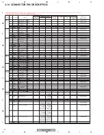
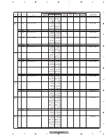
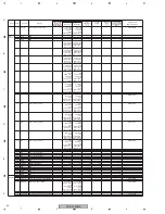
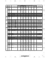
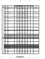
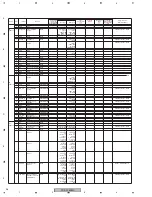
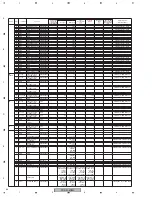
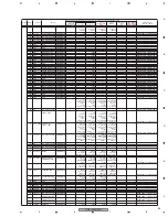
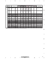
Name
MAIN POWER "ON"
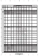
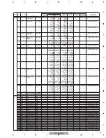
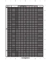
Basic operation(Numerical unit:Vdc; except for case when units are individually indicated)
No signal
With signal
"Signal direction
(DR : Data Relay)"
"AC power ON
(Power cord
connected to the
wall outlet) "
"AC Power OFF
(Power cord pulled
out of the wall outlet
"
"Power
management
"
Standby
"Main power
OFF
"
Pin name
Pin No.
AD1
CN8501
AD2
CN8502
3
1
2
3
4
5
6
7
8
9
10
11
12
13
14
15
16
17
18
19
20
21
22
23
24
25
26
27
28
29
30
31
32
33
1
2
3
4
6
7
8
9
F_ALM
GND
GND
GND
RE+
RE-
RD+
RD-
RCLK+
RCLK-
GND
RC+
RC-
RB+
RB-
RA+
RA-
GND
NC
NC
NC
NC
NC
NC
GND
MSEL
POWER
STB_MUTE
RFU
STATUS
GND
GND
GND
GND
GND
GND
P_ST_B
MR_ST_B
MR_RXD
NC
AC_DET_B
NC
Fan lock detect signal output
GND
GND
GND
Video system output E+
Video system output E-
Video system output D+
Video system output D-
Video system output clock+
Video system output clock-
GND
Video system output C+
Video system output C-
Video system output B+
Video system output B-
Video system output A+
Video system output A-
GND
Non-connection termial
Non-connection termial
Non-connection termial
Non-connection termial
Non-connection termial
Non-connection termial
GND
Module function grade select signal
POWER ON SIGNAL
Stand by power control signal
GND
Non-connection termial
GND
GND
GND
GND
GND
GND
Connecting detection (PDP
MAIN)
Connecting detection (MAIN
PDP)
UART data (PDP
MAIN)
Non-connection termial
AC power detection from power supply
Non-connection termial
0
0
0
0
0
0
0
0
0
0
0
0
0
0
0
0
0
0
-
-
-
-
-
-
0
0
0
0
0
-
0
0
0
0
0
0
0
0
0
-
0
-
0V during
normal Fan
operation;
3.3Vdc
while the fan is
stopped
0
0
0
Video mode
LVDS serial
differential E+
output 0Vac;
Bias 1.1Vdc
Video mode
LVDS serial
differential E-
output 0Vac;
Bias 1.4Vdc
Video mode
LVDS serial
differential D+
output 0Vac;
Bias 1.1Vdc
Video mode
LVDS serial
differential D-
output 0Vac;
Bias 1.4Vdc
Video data
clock
LVDS serial
differential
clock+
output 0.3Vac;
Bias 1.25Vdc
Video data
clock LVDS
serial
differential
clock-
output 0.3Vac;
Bias 1.25Vdc
0
Video
data LVDS
serial
differential C+
output 0.3Vac:
Bias 1.25Vdc
Video
data LVDS
serial
differential C-
output 0.3Vac:
Bias 1.25Vdc
Video
data LVDS
serial
differential B+
output 0Vac:
Bias 1.1Vdc
Video
data LVDS
serial
differential B-
output 0Vac:
Bias 1.4Vdc
Video
data LVDS
serial
differential A+
output 0Vac:
Bias 1.1Vdc
Video
data LVDS
serial
differential A-
output 0Vac:
Bias 1.4Vdc
0
-
-
-
-
-
-
0
0
3.3V
0
0
-
0
0
0
0
0
0
0
0
Clock signal
(3.3Vac) when
data
are received;
3.3Vdc
when no data
are received.
-
0
-
0V during
norma Fan
operation;
3.3Vdc
while the fan is
stopped
0
0
0
Video mode
LVDS serial
differential E+
output 0.3Vac;
Bias 1..25Vdc
Video mode
LVDS serial
differential E-
output 0.3Vac;
Bias 1..25Vdc
Video mode
LVDS serial
differential D+
output 0.3Vac;
Bias 1.25Vdc
Video mode
LVDS serial
differential D-
output 0.3Vac;
Bias 1.25Vdc
Video data
clock
LVDS serial
differential
clock+
output 0.3Vac;
Bias 1.25Vdc
Video data
clock LVDS
serial
differential
clock-
output 0.3Vac;
Bias 1.25Vdc
0
Video
data LVDS
serial
differential C+
output 0.3Vac:
Bias 1.25Vdc
Video
data LVDS
serial
differential C-
output 0.3Vac:
Bias 1.25Vdc
Video
data LVDS
serial
differential B+
output 0.3Vac:
Bias 1..25Vdc
Video
data LVDS
serial
differential B-
output 0.3Vac:
Bias 1.25Vdc
Video
data LVDS
serial
differential A+
output 0.3Vac:
Bias 1..25Vdc
Video
data LVDS
serial
differential A-
output 0.3Vac:
Bias 1.25Vdc
0
-
-
-
-
-
-
0
0
3.3V
0
0
-
0
0
0
0
0
0
0
0
Clock signal
(3.3Vac) when
data
are received;
3.3Vdc
when no data
are received.
-
0
-
0
0
0
0
0
0
0
0
0
0
0
0
0
0
0
0
0
0
-
-
-
-
-
-
0
0
3.3V
0
0
-
0
0
0
0
0
0
0
0
0
-
0
-
0
0
0
0
0
0
0
0
0
0
0
0
0
0
0
0
0
0
-
-
-
-
-
-
0
0
3.3V
0
0
-
0
0
0
0
0
0
0
0
0
-
0
-
0
0
0
0
0
0
0
0
0
0
0
0
0
0
0
0
0
0
-
-
-
-
-
-
0
0
0
0
0
-
0
0
0
0
0
0
0
0
0
-
0
-
0
0
0
0
0
0
0
0
0
0
0
0
0
0
0
0
0
0
-
-
-
-
-
-
0
0
0
0
0
-
0
0
0
0
0
0
0
0
0
-
0
-
FAN
MAIN
-
-
-
MAIN
PDP
MAIN
PDP
MAIN
PDP
MAIN
PDP
MAIN
PDP
MAIN
PDP
-
MAIN
PDP
MAIN
PDP
MAIN
PDP
MAIN
PDP
MAIN
PDP
MAIN
PDP
-
-
-
-
-
-
-
-
-
MAIN
PDP
-
-
-
-
-
-
-
-
PDP
MAIN
MAIN
PDP
PDP
MAIN
-
PDP
MAIN
-
Function
Summary of Contents for PDP-42MXE10
Page 9: ...PDP 425CMX 9 5 6 7 8 5 6 7 8 C D F A B E ...
Page 27: ...PDP 425CMX 27 5 6 7 8 5 6 7 8 C D F A B E ...
Page 37: ...PDP 425CMX 37 5 6 7 8 5 6 7 8 C D F A B E ...
Page 129: ...PDP 425CMX 129 5 6 7 8 5 6 7 8 C D F A B E ...
Page 132: ...PDP 425CMX 132 1 2 3 4 1 2 3 4 C D F A B E MAIN PWB CONNECTOR WAVE FORM POINT SIDE B ...

