background image


PDP-435PE

16

1

2

3

4

1

2

3

4

C

D

F

A

B

E

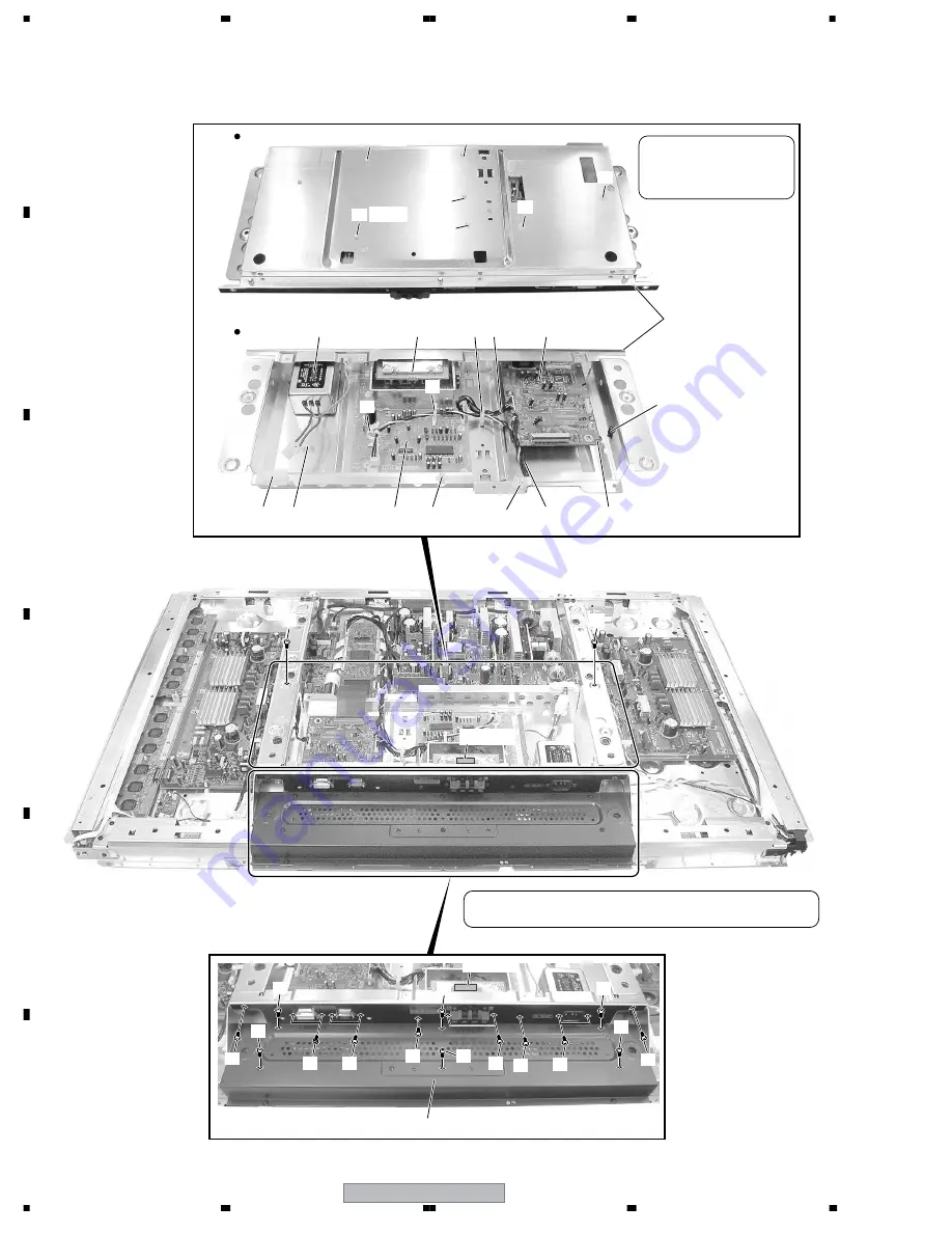
2.5  MULTI BASE SECTION

Back side

Front side

Note: 
The No. 12 parts must be 
inserted from the front 
surface.

10

7

12

12

9

1

3

13

13

4

6

15

16

5

15

2

11

14

15

9

12

12

12

17

17

17

21 17

8

17

18

19

17

17

17

17

20

17

17

17

17

20

(Note)

(Note)

(Note) (Note)

(Note)

(Note)

Note: When servicing, be sure to glue on the Gasket (AU)

and make sure that they won't peel off.

Summary of Contents for PDP-435PE

Page 1: ...EER CORPORATION 2004 PDP 435PE ARP3211 PLASMA DISPLAY PDP 435PE PRO 435PU THIS MANUAL IS APPLICABLE TO THE FOLLOWING MODEL S AND TYPE S This service manual should be used together with the following manual s Model Type Power Requirement Remarks PDP 435PE WYVI AC220 240V PDP 435PE WYVIXK AC220 240V PRO 435PU KUC AC120V Model No Order No Remarks PDP 435PE PRO 435PU ARP3212 SCHEMATIC DIAGRAM PCB CONN...

Page 2: ... adjustment and compartment covershields isolation resistor capacitor etc 3 When service is required observe the original lead dress Extra precaution should be taken to assure correct lead dress in the high voltage circuitry area 4 Always use the manufacture s replacement components Especially critical components as indicated on the circuit diagram should not be replaced by other manufacture s Fur...

Page 3: ... Any current measured must not exceed 0 5mA ANY MEASUREMENTS NOT WITHIN THE LIMITS OUTLINED ABOVE ARE INDICATIVE OF A POTENTIAL SHOCK HAZARD AND MUST BE CORRECTED BEFORE RETURNING THE SET TO THE CUSTOMER PRODUCT SAFETY NOTICE Many electrical and mechanical parts in PIONEER set have special safety related characteristics These are often not evident from visual inspection nor the protection afforded...

Page 4: ...cribed above If the places are touched there is a risk of electric shock 1 POWER SUPPLY Unit 215V 2 43 X DRIVE Assy 235V to 215V 3 43 Y DRIVE Assy 345V 4 43 SCAN A Assy 345V 5 43 SCAN B Assy 345V 6 X CONNECTOR AAssy 235V to 215V 7 X CONNECTOR B Assy 235V to 215V Part is the High Voltage Generating Points other than the Charged Section Part is Charged Section POWER SUPPLY Unit 43 Y DRIVE Assy 43 SC...

Page 5: ...the product Please check that neither solder debris nor screws remain inside the product 8 There should be no semi broken wires scratches melting etc on the coating of the power cord Damaged power cords may lead to fire accidents so please be sure that there are no damages If you find a damaged power cord please exchange it with a suitable one 9 There should be no spark traces or similar marks on ...

Page 6: ... ASSY 31 3 1 6 HD AUDIO AMP ASSY 33 3 2 WAVEFORMS 34 PCB CONNECTION DIAGRAM Refer to Service Manual ARP3212 5 PCB PARTS LIST 38 6 ADJUSTMENT 46 6 1 ADJUSTMENT REQUIRED WHEN THE SET IS REPAIRED OR REPLACED 46 6 2 DRIVE ASSY ADJUSTMENT 47 6 3 COMMAND 48 6 3 1 RS232C COMMAND 48 6 4 METHOD FOR REPLACING THE SERVICE PANEL ASSY 56 7 GENERAL INFORMATION 57 7 1 DIAGNOSIS 57 7 1 1 PCB LOCATION 57 7 1 2 DIA...

Page 7: ...umber of Pixels Audio Amplifier Surround System Power Requirement 120V AC 60Hz 298W 0 2W Standby Dimensions Weight Model PRO 435PU 1024 x 768 pixels 13 W 13 W 1kHz 10 8Ω SRS FOCUS TruBass 1120 W x 652 H x 93 D mm 44 1 8 W x 25 11 16 H x 3 7 8 D inches 26 8 kg 59 1 lbs 43 Plasma Display Wiping Cloth x1 Speed Clamp x3 Bead Bands x3 Binder Assy AEC1908 Speaker Cushion x1 AEB1384 AED1208 Power Cord Ac...

Page 8: ...part Therefore when replacing be sure to use parts of identical designation Screws adjacent to mark on product are used for disassembly For the applying amount of lubricants or glue follow the instructions in this manual In the case of no amount instructions apply as you think it appropriate NOTES 14 13 3 1 4 7 10 8 9 18 15 6 16 17 15 5 12 11 16 3 4 17 20 19 19 1 2 14 13 10 8 9 6 7 12 11 3 4 18 PR...

Page 9: ...ontrast table 2 Mark No Description Part No Mark No Symbol and Description PDP 435PE WYVI PDP 435PE WYVIXK PRO 435PU KUC 1 Power Cord ADG1214 ADG1214 Not used 2 Power Cord Not used Not used ADG1215 5 Code Case AHC1041 AHC1049 Not used 6 Center Pad 43 Not used AHA2336 Not used NSP 7 Warranty Card ARY1114 ARY1114 ARY1134 8 Mirror Mat AHG1284 AHG1327 AHG1284 9 Pad 43T L AHA2362 Not used AHA2362 9 Pad...

Page 10: ... side Upper side 32 29 9 5 28 23 23 24 23 23 23 23 23 34 34 34 4 7 6 33 23 23 23 21 24 26 26 25 25 25 25 31 22 22 28 28 2 35 14 22 13 27 27 27 12 10 23 23 23 24 23 1 23 23 30 30 8 22 27 11 27 20 19 22 27 15 16 27 17 18 27 31 3 31 31 3 25 25 33 33 33 33 33 33 33 33 33 33 ...

Page 11: ...ble J203 ADD1217 14 Flexible Cable J204 ADD1218 15 Flexible Cable J205 ADD1219 16 Flexible Cable J206 ADD1220 17 Flexible Cable J207 ADD1221 18 Flexible Cable J208 ADD1222 19 Flexible Cable J209 ADD1223 20 Flexible Cable J210 ADD1224 21 Y Drive Protect Sheet AMR3346 22 Flat Clamp AEC1879 23 PCB Spacer AEC1941 24 PCB Support AEC1938 25 PCB Spacer AEC1944 26 PCB Support AEC1958 27 Wire Saddle AEC174...

Page 12: ...PDP 435PE 12 1 2 3 4 1 2 3 4 C D F A B E 2 3 CHASSIS SECTION 2 Upper side Upper side 13 13 15 15 15 14 12 11 12 11 10 9 14 14 14 15 16 15 15 16 13 6 13 7 4 5 8 1 3 2 ...

Page 13: ...IVE Assy AWV2078 4 Wire A J101 ADX2839 5 11P Housing Wire J102 ADX2840 6 12P Housing Wire J103 ADX2921 7 9P Housing Wire J106 ADX2923 8 3P Housing Wire J109 ADX2847 9 SUB Frame L Assy 43P ANG2545 10 SUB Frame R Assy 43P ANG2548 11 Wire Saddle AEC1745 12 Edging Saddle AEC1737 13 Screw ABZ30P060FTC 14 Screw AMZ30P080FTC 15 Screw VBB30P080FNI 16 Screw PMB30P060FNI ...

Page 14: ...35PE 14 1 2 3 4 1 2 3 4 C D F A B E 2 4 FLAME SECTION Upper side Upper side Upper side 17 10 11 5 14 13 18 1 4 3 18 15 2 12 17 17 17 17 17 17 16 16 17 15 15 15 6 8 9 17 17 17 17 17 16 16 17 15 15 15 7 17 17 ...

Page 15: ...ng Wire 43 J110 ADX2848 5 Flexible Cable J211 ADD1225 6 Front Chassis HU Assy 43 ANA1787 7 Front Chassis HD Assy 43 ANA1788 8 Front Chassis VL 43 ANA1790 9 Front Chassis VR 43 ANA1791 10 Clamp AEC1884 11 Flat Clamp AEC1879 12 Switch Holder AMR3402 13 IR Holder ANG2665 14 Wire Clip AEC1948 15 Screw BPZ30P080FTB 16 Screw AMZ30P080FTC 17 Screw AMZ30P060FTB 18 Screw ABZ30P060FTC ...

Page 16: ...he No 12 parts must be inserted from the front surface 10 7 12 12 9 1 3 13 13 4 6 15 16 5 15 2 11 14 15 9 12 12 12 17 17 17 21 17 8 17 18 19 17 17 17 17 20 17 17 17 17 20 Note Note Note Note Note Note Note When servicing be sure to glue on the Gasket AU and make sure that they won t peel off ...

Page 17: ...P Housing Wire J104 ADX2922 6 13P Housing Wire J105 ADX2843 7 Multi Base P Assy ANA1786 8 Under Cover Assy ANG2589 9 Locking Card Spacer V0 AEC2005 10 Edge Saddle AEC1946 11 Clamp AEC1884 12 PCB Spacer AEC1941 13 HL 18 AEC1980 14 SB Spacer AEC2002 15 Wire Saddle AEC1745 16 Screw PMB30P060FNI 17 Screw AMZ30P060FTB 18 Hexagon Headed Screw BBA1051 19 Screw PMZ26P060FTB 20 Gasket AU ANK1745 21 Screw B...

Page 18: ...ark No Description Part No 1 Rear Case 43P ANE1625 2 Inner Grip Assy AMR3434 NSP 3 Name Label See Contrast table 2 4 Volt caution Label See Contrast table 2 5 Terminal Label See Contrast table 2 6 Screw ABZ30P100FTB 7 Serial Sheet AAX3143 8 Screw AMZ30P060FTB Mark No Description Part No Mark No Symbol and Description PDP 435PE WYVI PDP 435PE WYVIXK PRO 435PU KUC NSP 3 Name Label AAL2567 AAL2571 AA...

Page 19: ...6 1 Mark No Description Part No 1 PANEL KEY Assy AWZ6843 2 Front Case Assy See Contrast table 2 3 Power Button AAD4127 NSP 4 Panel Holder V 43 ANG2661 NSP 5 Panel Holder Assy 43 ANG2674 6 Coil Spring ABH1114 7 Blind Cushion AEB1383 8 Screw ABZ30P060FTC Mark No Description Part No Mark No Symbol and Description PDP 435PE WYVI PDP 435PE WYVIXK PRO 435PU KUC 2 Front Case Assy 43PE AMB2833 AMB2833 Not...

Page 20: ...NSP Tape ZTC POLYCA 20 NSP Tape ZTC 900UL 15 NSP Silicone Rubber ZTX HC20 15 NSP Silicone Rubber ZTX HC50 15 NSP Wiping Cloth ZTX MX100 13 NSP Film ZTX 2102Y35 2R5 NSP Film ZTX 2102Y45 5 Mark No Description Part No Mark No Description Part No NSP 1 43 ADDRESS Assy AWV2076 NSP 2 43 ADDRESS Assy AWZ6862 NSP 1 43 SCAN Assy AWV2079 NSP 2 43 SCAN A Assy AWZ6873 NSP 2 43 SCAN B Assy AWZ6874 NSP 2 X CONN...

Page 21: ...Z30P080FZB NSP 1 Front Case Assy 435SVC AMB2841 2 Panel Cushion H 43 AED1255 2 Panel Cushion V 43 AED1256 NSP 2 Front Case 43P AMB2821 1 Rear Case 43P ANE1612 NSP 1 Vinyl Pouch AHG 195 1 Pad 43T L AHA2362 1 Pad 43T R AHA2363 1 Pad 43B L AHA2364 1 Pad 43B R AHA2365 1 Carton 43 AHD3165 1 Upper Carton 435SVC AHD3267 1 Protect Sheet AHG1331 Note 1 The one provided with the AHG 195 is not used Note 2 T...

Page 22: ...ignal 5V 5V 5V Drive Signal Drive Signal Drive Signal 16 5V 16 5V 16 5V 6 5V 16 5V VSUS V_IC5V VCC_VH V_OFS VC_VF VC_VF 5V VSUS ADD SEL_PULSE IC3202 VCC _VH IC5V ADD SEL_PULSE IC3203 MASK MOD IC2307 5V 16 5V 16 5V VSUS 5V V_OFS V_IC5V MASK MOD IC2303 SOFT D BLOCK REGULATOR DC_DC CONV BLOCK LOGIC BLOCK SUB FILD CONV XY DRV SEQUENCE PATTERN GEN IC5401 PEG054A RESONANCE BLOCK FLASH MEMORY IC5305 MODU...

Page 23: ...43 ADDRESS ASSY X1 X2 X CONNECTOR A ASSY X CONNECTOR B ASSY HD SP TERMINAL ASSY HD AUDIO AMP ASSY 43 X DRIVE ASSY 5V 5V 5V Drive Signal Drive Signal 16 5V 16 5V 16 5V VSUS V_RN 5V 6 5V V_RN MASK MOD IC1203 5V 9V 16 5V VSUS MASK MOD IC1207 REGULATOR DC_DC CONV BLOCK LOGIC BLOCK RESONANCE BLOCK RESET PULSE BLOCK PSUS PSUS VSUS SUS OUT SUS OUT TMDS RECEIVER IC4202 EEPROM for Backup Bus Buffer Bus Buf...

Page 24: ...S MSK YOFS YSUS PD SCN_5V_PD Y_DD_PD SCAN_PD YDRIVE_PD 16 5V DGND 6 5V DGND N C N C VSUS VSUS 215V VH OVP VOFS UVP VH UVP VSUS N C SUSGND SUSGND VH 5V VSUS VH IC5V CN2101 CN2102 IC2305 5V IC5V VH VF Y2 Y3 Y1 VOFS OVP VOFS IC5V UVP VF IC2202 L2204 L2205 YSUS U2 YSUS D2 HB DRIVER XSUS P D Circuit Photo Coupler 5V VSUS To SCAN ASSY To 43 SCAN A ASSY From DIGITAL VIDEO ASSY From POWER SUPPLY UNIT To 4...

Page 25: ... D XNR D XSUS_PD XDD_PD XDRV_PD 16 5V DGND 6 5V DGND N C N C VSUS VSUS 215V VSUS VRN UVP P D VRN OVP P D VSUS N C SUSGND SUSGND 5V CN1201 IC1205 5V X1 X2 N C IC1101 L1102 L1103 XSUS U2 XSUS D2 HB DRIVER XSUS P D Circuit Photo Coupler 5V VCP VSUS PSUS To X CONNECTOR ASSY From DIGITAL VIDEO ASSY From POWER SUPPLY UNIT 5V 16 5V VSUS 5V 16 5V IC1102 IC1202 Charge Pump Circuit D D CONV T1401 L1104 L110...

Page 26: ...V 9 KEY_B 14 REM_B 15 STB_MT 13 AUDIO_R 20 AUDIO_L REM KEY LED R LED G 6 DDC_SCL 7 DDC_SDA 14 DDC_ 5V CN4003 CN4002 CN4004 CN4009 R3 R2 R4 R7 R8 DVI CONNECTOR MDR CONNECTOR IC4006 BUF IC4006 BUF IC4006 BUF IC4006 BUF Q4004 INV Q4006 INV Q4009 INV Q4006 INV Q4007 Q4011 NOR IC4006 BUF Q4006 INV Q4011 INV L_IN R_IN LED_G_B LED_R_B REM_B KEY_B MR_AC_OFF REQ_MD MR_ST_B B_SCL B_SDA TXD0 RXD0 DVI_OFF DVI...

Page 27: ...tion key code signal output at panel side 0 3 3V amplitude square wave at key operation 10 MR_ST_B I Connection state detecting signal with the MR 0VDC 11 MTXD I UART communication receive data with the main UCOM external PC at the MR side 0 3 3V amplitude square wave 12 GND GND 13 AUDIO_R I R ch audio signal input Audio R signal 14 REM_B O Remote control code signal output 0 3 3V amplitude square...

Page 28: ... O Standby signal of the audio block 3 3V DC 8 A_MUTE O Audio mute signal input 0V DC 9 SCL O I2C control signal for audio 0 3 3V amplitude square wave 10 SDA O I2C control signal for audio 0 3 3V amplitude square wave 11 FOCUS O Focus function control signal 3 3V DC 12 SRS O SRS function control signal 3 3V DC 13 TRUBASS O TRUBASS function control signal 3 3V DC No Signal Name I O Signal Descript...

Page 29: ... 8bit video signal output RED even number 0 3 3V amplitude square wave 30 RA1 O 8bit video signal output RED even number 0 3 3V amplitude square wave 31 RA2 O 8bit video signal output RED even number 0 3 3V amplitude square wave 32 RA3 O 8bit video signal output RED even number 0 3 3V amplitude square wave 33 RA4 O 8bit video signal output RED even number 0 3 3V amplitude square wave 34 RA5 O 8bit...

Page 30: ...Power supply 3 3V output of module UCOM at panel side 3 3VDC 85 B_SDA I E2PROM control signal for backup 0 3 3V amplitude square wave 86 RXD0 O UART communication receive data with the main UCOM external PC at MR side 0 3 3V amplitude square wave 87 REM_B O Remote control code signal output 0 3 3V amplitude square wave at remocon code transmission 88 TXD0 I UART communication transmission data wit...

Page 31: ...tal AND BUSY RXD1 CLK1 CNVSS TXD1 PANEL SIZE PSIZE XSUSA XSUSB SCAN Connector disconnection detection Vrst 8bit DAC Vofs YDRV_ UC XDRV_ UC AC_ DET AC OFF Det STB_ MT MRAC_ DET B_ SCL B_ SDA VOFS VSUS VD_ IN PSW _ D DIGITAL VIDEO ASSY IC5201 HD VD CLK DE 43 Y DRIVE ASSY 43 X DRIVE ASSY PANEL SENSOR ASSY 43 ADDRESS ASSY x8 SCAN ASSY POWER SUPPLY ASSY CN5001 CN4001 From PANEL IF ASSY From PANEL IF AS...

Page 32: ..._PD I Power down detecting signal of POWER SUPPLY block 0VDC 8 RELAY O Relay control signal 3 3VDC 9 DRF O Drive control signal 0VDC 10 AC_DET I Primary side power AC state output at panel side 3 0VDC 11 PD_TRIGGER I Power down trigger 3 3VDC No Signal Name I O Signal Description Voltages at NTSC Signal Input 1 VADR I Address drive power 61V input 61VDC 2 VADR I Address drive power 61V input 61VDC...

Page 33: ...Audio A2 SCL SDA ST BY A1 A3 SRS FOCUS TRUBASS A_NG_B WOW IC IC3501 VOLUME IC IC3502 DC DETECT BLOCK BUFFER 9 0V 9 0V 16 5V 16 5V 9 0V 16 5V R_OUT R_OUT L_OUT L_OUT HD SP TERMINAL ASSY HD AUDIO AMP ASSY J3701 CN3503 CN3501 CN3504 From PANEL IF ASSY From POWER SUPPLY Unit REGULATOR IC3503 POWER AMP IC IC3504 ...

Page 34: ...H 4µsec div CH1 CH2 2 CH1 TP5102 VD CH2 TP5103 DE V 2V div H 2msec div CH1 CH2 2 CH1 TP5102 VD CH2 TP5103 DE V 2V div H 4µsec div CH1 CH2 3 CH1 TP5101 HD CH2 TP5103 DE V 2V div H 2µsec div CH1 CH2 3 CH1 TP5101 HD CH2 TP5103 DE V 2V div H 40nsec div CH1 CH2 4 CH1 TP5101 HD CH2 CN5001 pin 77 DCLK V 2V div H 40nsec div CH1 CH2 5 CH1 TP5102 VD CH2 CN5001 pin 86 RA_IN2 V 2V div H 2msec div CH1 CH2 ...

Page 35: ...c div CH1 CH2 1 CH1 K4005 VDI CH2 K4006 HDI V 2V div H 10µsec div CH1 CH2 2 CH1 K4005 VDI CH2 CN4004 pin 29 RAO V 2V div H 5msec div CH1 CH2 3 CH1 K4006 HDI CH2 K4003 DEI V 2V div H 5µsec div CH1 CH2 4 CH1 K4003 DEI CH2 K4002 DCLK V 2V div H 5µsec div CH1 CH2 4 CH1 K4003 DEI CH2 K4002 DCLK V 2V div H 10nsec div CH1 CH2 ...

Page 36: ... Sustain Waveform CH2 K2016 YSUS G K2010 DGND CH3 K2025 YSUS U1 K2010 DGND CH4 K2022 YSUS U2 K2010 DGND CH5 K2026 YSUS B K2010 DGND CH6 K2024 YSUS D2 K2010 DGND CH7 K2027 YSUS D1 K2010 DGND 43 Y DRIVE ASSY V 1V div H 500nsec div CH2 CH3 CH4 CH5 CH6 CH7 Control Signal Sustain Waveform Gen CH2 K2006 SI K2029 DGND CH3 K2009 OC1 K2029 DGND CH4 K2004 OC2 K2029 DGND CH5 K2007 CLR K2029 DGND CH6 K2003 CL...

Page 37: ...2 pin 4 ADR_U2 CH4 Q1602 pin 2 ADR_D2 V 10V div Input VIDEO Signal Color bar CH2 H 2msec div CH3 CH4 CH2 CH3 CH4 4 H 500nsec div CH1 Q1601 Drain V ADR CH2 Q1603 Source CH3 Q1602 Source V 10V div Input VIDEO Signal Color bar CH1 H 2msec div CH2 CH3 CH1 CH2 CH3 5 H 500nsec div CH1 Q1601 Drain V ADR CH2 Q1603 Source CH3 Q1602 Source V 10V div Input VIDEO Signal B W 1 8 CH1 H 2msec div CH2 CH3 CH1 CH2...

Page 38: ...2073 2 PANEL IF ASSY AWZ6841 1 DIGITAL VIDEO ASSY AWV2074 NSP 1 HD AUDIO ASSY AWV2075 2 HD AUDIO AMP ASSY AWZ6863 2 HD SP TERMINAL ASSY AWZ6864 NSP 1 43 X DRIVE ASSY AWV2077 2 PANEL LED ASSY AWZ6842 2 PANEL KEY ASSY AWZ6843 2 KEY CONTROL ASSY AWZ6844 2 PANEL IR ASSY AWZ6845 2 43 X DRIVE ASSY AWZ6865 2 PANEL SENSOR ASSY AWZ6872 1 43 Y DRIVE ASSY AWV2078 1 POWER SUPPLY UNIT AXY1085 Mark No Descripti...

Page 39: ... CCSRCH181J50 C3261 CCSRCH181J50 C3205 C3210 C3216 C3221 CCSRCH331J50 C3230 C3231 C3241 C3242 C3248 CCSRCH331J50 C3254 C3260 C3265 CCSRCH331J50 C3208 C3209 C3219 C3220 C3227 CCSRCH390J50 C3229 C3238 C3240 C3252 C3253 CCSRCH390J50 C3263 C3264 CCSRCH390J50 C3202 C3213 C3224 C3235 C3246 CKSRYB105K6R3 C3257 CKSRYB105K6R3 Mark No Description Part No RESISTORS R3202 R3210 R3216 R3224 R3229 RAB4C221J R32...

Page 40: ...ACH1357 C5205 CKSRYB472K50 Mark No Description Part No C5206 C5223 C5231 C5245 C5252 CKSSYB102K50 C5257 C5260 CKSSYB102K50 C5202 C5204 C5207 C5208 CKSSYF104Z16 C5210 C5212 C5218 C5224 CKSSYF104Z16 C5226 C5227 C5243 C5244 CKSSYF104Z16 RESISTORS R5209 R5211 R5212 R5235 RAB4C101J R5254 R5255 R5265 R5266 RAB4C101J R5205 RAB4C103J R5270 R5271 RAB4C472J R5256 R5257 RAB4C474J R5294 RS1 16S0R0J Other Resi...

Page 41: ...EAT330M25 C3566 CEHAT101M10 C3561 CEHAT101M16 C3562 C3565 CEHAT220M50 C3559 C3560 CEHAT2R2M50 Mark No Description Part No C3509 CEHAT331M16 C3507 CEHAT471M25 C3571 CEHAT472M25 C3563 CEHATR47M50 C3512 C3522 C3572 CFTLA103J50 C3511 C3513 C3518 C3533 C3534 CFTLA104J50 C3545 C3548 C3573 C3576 CFTLA104J50 C3521 CFTLA333J50 C3524 CFTLA334J50 C3523 CFTLA474J50 C3506 C3508 C3510 C3527 C3535 CKSRYB103K50 C...

Page 42: ...101 DRIVE HEATSINK ANH1628 1101 SCREW PMH30P080FTC 43 X SUS BLOCK SEMICONDUCTORS IC1203 IC1207 STK795 510 IC1202 HCPL M611 IC1205 NJM2872F05 IC1206 TND301S IC1204 IC1209 TND307TD Mark No Description Part No Q1209 2SA1727 Q1203 2SD1898 Q1205 2SK2865 Q1208 DTC124EUA Q1201 HN1B04FU D1212 1SS302 D1211 D1213 1SS355 D1204 D1217 D1FL40 D1201 D1207 EC10QS04 D1208 UDZS5R6 B COILS AND FILTERS L1204 L1205 AT...

Page 43: ...M200NA4 X4851 CERALOCK ASS1162 Mark No Description Part No PANEL IR ASSY SEMICONDUCTORS Q4901 2SC4116 D4902 DA204U CAPACITORS C4901 CEVW470M6R3 C4902 CKSRYB103K50 C4903 CKSSYB102K50 C4904 CKSSYF104Z16 RESISTORS Other Resistors RS1 16SS J OTHERS CN4901 L PLUG 3P KM200NA3L U4901 IR UNIT RPM7240 H5 PANEL SENSOR ASSY SEMICONDUCTORS IC1072 MM1522XU IC1071 MM3012XN CAPACITORS C1071 C1074 C1075 CKSRYB103...

Page 44: ...C2205 C2216 C2217 CCSRCH331J50 C2203 C2218 CKSRYB105K6R3 C2230 C2232 C2233 C2235 CKSSYB104K10 C2201 C2208 C2215 C2219 CKSYB105K25 RESISTORS Mark No Description Part No R2240 R2241 RS1 10S1003F R2244 R2247 RS1 10S100J R2260 R2261 RS1 10S220J R2205 R2211 R2213 R2220 R2221 RS1 10S2R2J R2253 R2265 RS1 10S2R2J R2234 RS1 16S1002F R2235 RS1 16S4701F R2233 R2242 RS1 16S8201F R2215 R2230 RS1MMF101J R2256 R...

Page 45: ...7 D2438 UDZS33 B D2432 UDZS4R3 B D2423 D2431 UDZS5R6 B COILS AND FILTERS T2402 ATK1156 T2403 ATK1157 T2401 ATK1158 L2402 LFEA100J L2401 LFEA101J L2403 LFEA470J CAPACITORS C2406 ACH1360 C2401 ACH1361 C2427 CEHAT100M50 C2403 CEHAT101M16 C2405 C2407 C2417 CEHAT101M25 C2414 CEHAT221M16 C2410 CEHAT221M25 C2411 CEHAT331M25 C2420 CEHAT470M2A C2409 C2419 CKSRYB103K50 Mark No Description Part No C2402 C241...

Page 46: ...ings 3 Use a stable AC power supply 43 Y DRIVE Assy No adjustment required POWER SUPPLY Unit No adjustment required DIGITAL VIDEO Assy Writing of backup data is required Refer to the 7 1 7 BACKUP WHEN THE MAIN UNIT IS ADJUSTED 43 X DRIVE Assy No adjustment required Other assemblies No adjustment required Service Panel Refer to the 6 4 METHOD FOR REPLACING THE SERVICE PANEL ASSY POWER SUPPLY Unit D...

Page 47: ...ystem Specified values for adjustment and adjustment points Note Connect GND of the probe with DGND DGND X Drive Assy K1020 Y Drive Assy K2010 for input signal For outputting a signal obtain a signal from the FET gate terminal For adjustment magnify any pulse in the waveform VGS 5V line Magnify 500us div 50ns div Input signal 1V div Output FET VGS 5V div Assy Replaced IC Signal for which Readjustm...

Page 48: ...5 special communication device when the Media Receiver is not connected with the PDP Note The special communication device for the PDP 503P cannot be used with this unit because the control lines within the MDR cable are different Connection GGF1475 special communication device MDR D SUB 9 pin straight cable PC for control Connect to the D SUB 9 pin connector Communication line Connect the system ...

Page 49: ...PDP 435PE 49 5 6 7 8 5 6 7 8 C D F A B E Schematic diagram of the special communication device ...

Page 50: ...de to 60 Hz VIDEO Setting the frequency in Mask mode to 60 Hz PC Setting the frequency in Mask mode to 70 Hz PC Setting the frequency in Mask mode to 72 Hz VIDEO Setting the frequency in Mask mode to 75 Hz VIDEO Turning the FOCUS function off Turning the FOCUS function on Obtaining various adjustment values Obtaining the serial no of the panel Obtaining the power down point log Obtaining the panel...

Page 51: ... Negative positive inversion display Panel white balance adjustment Blue highlight Panel white balance adjustment Blue low light Setting input signal type to video Setting input signal type to PC The PD signal is not passed through the POWER SUPPLY Assy The PD signal is passed through the POWER SUPPLY Assy Panel white balance adjustment Green highlight Panel white balance adjustment Green low ligh...

Page 52: ...information on the unit such as the software version GS2 Obtaining information on the status of the unit GSD Obtaining information on shutdown GAJ Obtaining data on ABL setting values electronic control adjustment values and drive system adjustment values Note Ignore the 2 byte checksum at the end Order Data Size Remarks 1 ABL table currently used 3 bytes AB1 AB3 2 ABL adjustment value 3 bytes 000...

Page 53: ... data 1 byte 0 D or F 15 Data of hour meter for the fourth latest PD 7 bytes 1st 5th byte Hour 6th 7th byte Minute 16 Data on temperature for the fourth latest PD TEMP1 3 bytes 000 255 17 Fifth latest 1st PD data 1 byte 0 D or F 18 Fifth latest 2nd PD data 1 byte 0 D or F 19 Data of hour meter for the fifth latest PD 7 bytes 1st 5th byte Hour 6th 7th byte Minute 20 Data on temperature for the fift...

Page 54: ...er 1 Each time hour meter data are cleared the accumulated time data are updated The total for data items 15 and 16 is the total power on time after shipment The accumulated time of cleared hour meter data cannot be cleared 2 The hour meter data that indicate driving hours of the panel are displayed on the Factory menu Upon shipment the data are cleared Order Data Size Remarks 1 Notifying that the...

Page 55: ...SD data 1 byte 0 5 22 Sixth latest SD subcategory data 1 byte 0 3 23 Data of hour meter for the sixth latest SD 7 bytes 1st 5th byte Hour 6th 7th byte Minute 24 Data on temperature for the sixth latest SD TEMP1 3 bytes 000 255 25 Seventh latest SD data 1 byte 0 5 26 Seventh latest SD subcategory data 1 byte 0 3 27 Data of hour meter for the seventh latest SD 7 bytes 1st 5th byte Hour 6th 7th byte ...

Page 56: ... SET key Enter the value using the 2 or 3 key Using the MUTE key select the main item INFORMATION Select the subitem HOUR METER using the 5 or key and SET key Clear the hour meter data In the same way select the subitem PULSE METER PANEL SD or PANEL PD under the main item INFORMATION then clear the data Clearing various logs for the panel such as that for the hour meter It is necessary to clear va...

Page 57: ...DDRESS Assy 43 ADDRESS Assy X CONNECTOR B Assy 43 ADDRESS Assy PANEL SENSOR Assy POWER SUPPLY Unit DIGITAL VIDEO Assy 43 SCAN B Assy 43 Y DRIVE Assy 43 SCAN A Assy PANEL KEY Assy PANEL IR Assy PANEL IF Assy HD SP TERMINAL Assy HD AUDIO Assy PANEL LED Assy KEY CONTROL Assy 43 ADDRESS Assy 43 ADDRESS Assy X CONNECTOR A Assy 43 X DRIVE Assy Rear view ...

Page 58: ...n P power down P shutdown No backup copy Disconnection of the system cable Power management when the Media Receiver is not connected with the PDP RED MR LED PANEL LED GREEN RED GREEN RED GREEN RED GREEN RED GREEN RED GREEN RED GREEN RED GREEN RED GREEN RED GREEN RED GREEN RED GREEN Normal Abnormality in MR Abnormality in the panel Disconnection of cable 0 5s 1 0s 3 0s 3 0s 0 5s 0 5s 0 5s 3 0s 0 5s...

Page 59: ...aker cable Powering off Internal temperature is too high Check temperature around media receiver SD11 Lit 5 times Audio failure Shutdown 3 seconds after warning Powering off Internal protection circuits turns power off Is the speaker cable short circuited SD05 6 times Lit Communication failure of the module microcomputer Immediate shutdown 7 times Lit Main 3 wire serial communication in failure Im...

Page 60: ...n subcategory on the Factory menu DIGITAL VIDEO Communication failure of the EEPROM 4K MODULE UCOM BLOCK IC5206 PANEL IF Communication failure of the EEPROM 2K PANEL IF BLOCK IC4002 Disconnection of cable CN4009 CN3501 Check if the cable is disconnected or not securely connected HD AUDIO Defective volume IC HD AUDIO AMP Assy IC3502 Defective 114 pin FPC CN4004 CN5001 ADY1081 Check if the 114 pin F...

Page 61: ...SY upper DIGITAL VIDEO ASSY ADDRESS ASSY lower X DRIVE ASSY Y DRIVE ASSY POWER SUPPLY UNIT IC5208 PD MUTE circuit Block diagram of the power down signal system Note The figures 1 indicate the number of times the LED flashes on the panel when power down occurs in the corresponding route Relay control Protection circuit IC5201 module microcomputer Flashes in a case of power down other than power sup...

Page 62: ...C1203 IC1207 mask module IC1204 IC1206 R1230 IC1205 VRN OCP X SUS BLOCK Q1205 R1226 R1251 10 X DCDC 43 X DRIVE Assy VRN OVP VRN DC DC IC1403 IC1404 VRN UVP VRN DC DC IC1402 IC1403 IC1404 X SUS BLOCK Q1205 R1226 R1251 11 X SUS 43 X DRIVE Assy X RESONANCE BLOCK Q1102 Q1103 Q1114 Q1105 Q1108 Q1109 Q1111 Q1112 IC1101 IC1102 D1103 D1113 D1118 D1125 D1129 D1130 Control signal series resistors 12 DIG DCD...

Page 63: ... the PDP 435PE PRO 435PU are described here How to enter Factory mode using the remote control unit Power down log INFORMATION PANEL PD Please refer to the technical documentation Service knowhow is the same as G4 PDP models The last 8 power down records are held with the latest power down displayed at the top In the FIRST column the location where the PD circuit was activated first location indic...

Page 64: ...h TEMP 1 value PDP 435PE TEMP 1 value 195 74 C PRO 435PU TEMP 1 value 195 74 C N N I F O M R I N 1 0 1 3 N T V S T 1 A T I O 1 1 5 10 15 16 5 10 15 20 25 30 35 40 T E M P E R A T U R E T E M P 1 1 2 8 T E M P 2 1 4 9 1 F A N 2 5 Note To update the data on temperature use the Left and Right keys on the remote control unit Reference Serial number information INFORMATION SERIAL You can check the seri...

Page 65: ... sec for about 8 seconds then the unit shifts to Power Management mode the green LED lights Although the PC signal data are displayed for the PDP 434P series panels for the PDP 435P series panels this is not possible because the EDID ROM has not been provided As the connection conditions of the system cables MDR cable DVI cable are usually detected if no connection such as cable disconnection is d...

Page 66: ...he DRF RS232C command to turn the large signal system off 3 Send the DRN RS232C command to turn the large signal system on Notes As the unit enters Power Down and Muting On mode when Methods 1 and 2 are performed and power downs other than those caused by the power PS_PD and DC DC converter DIGITAL_DC DC circuits are not activated If the slide switch is set from OFF to ON while the power is on a p...

Page 67: ... VIDEO Assy is mounted on another unit reuse of the repaired DIGITAL VIDEO Assy The keyword of the DIGITAL VIDEO Assy to be reused must be changed to not adjusted using the UAJ RS232C command Note 1 If a repaired DIGITAL VIDEO Assy is mounted in another unit Unit 2 without this change of keyword and the power to the unit 2 is turned off the data in force before the repair of the DIGITAL VIDEO Assy...

Page 68: ...F ORMA T I ON V D 1 0 1 3 N T V S T 1 1 1 2 3 4 5 6 7 8 9 10 11 12 13 14 15 16 17 18 19 20 21 22 23 24 25 26 27 28 29 30 31 32 33 34 35 36 37 38 39 40 2 3 4 5 6 7 8 9 10 11 12 13 14 15 16 I D A D A A S F T T R R Y E S NO N E I G A L T E E P ROM I N F ORMA T I ON V D 1 0 1 3 N T V S T 1 Status confirmation Display the screen page shown below to check if the DIGITAL VIDEO Assy has been adjusted or a...

Page 69: ...ommand Check that the adjustment data have been changed 7 Change the keyword for the DIGITAL VIDEO Assy to adjusted by sending the FAJ RS232C command Note Use a Minolta CA 100 color difference meter or the equivalent for measurement Otherwise the specifications of the product cannot be assured Note To cancel adjusted data and return to the values before adjustment send the BCP RS232C command Turn ...

Page 70: ...ss was not performed when the Digital Assy was replaced See 7 1 7 Backup when the main unit is adjusted Cable disconnection CN4852 CN4010 Check if the cables are disconnected or not securely connected Check if a pulse is output when the key corresponding to Pin 8 of the CN4010 is pressed KEY CONTROL Defective KEY SCAN IC KEY CONTROL Assy IC4851 Check if a pulse is output when the key corresponding...

Page 71: ...ase Assy 43P PANEL KEY Assy 1 3 1 When reassembling first secure the screws for these holes to position the Rear Case 43P correctly 1 1 1 2 1 2 2 2 2 2 1 2 4 1 2 2 2 1 1 2 1 1 2 2 1 1 2 2 2 2 2 2 2 2 2 2 2 5 6 2 2 1 Note If you wish to remove only the Front Case Assy you can remove it in the order of 1 4 5 and 6 1 6 2 Secure the screws in the order of and Ÿ Then secure the screws on the upper side...

Page 72: ...d remove the wires 4 Remove the Switch Holder 5 Remove the three screws to remove the Front Chassis VR 43 6 Remove the seven screws 7 Remove the X CONNECTOR A and B Assy s X CONNECTOR A and B Assy s 2 43 X DRIVE Assy X CONNECTOR A Assy X CONNECTOR B Assy 5 5 5 1 2 2 3 4 7 7 6 4 6 3 PANEL LED Assy Flat Clamp Switch Holder Front Chassis VR 43 ...

Page 73: ...screws to remove the Front Chassis VL 43 5 Remove the four screws 6 Disconnect the two pin connectors 7 Remove the two PCB spacers 8 Remove the four edge card spacers 9 Remove the 43 SCAN A and B Assy s 43 SCAN A and B Assy s 3 43 Y DRIVE Assy 43 SCAN A Assy 43 SCAN B Assy 4 4 4 1 1 2 3 9 9 8 8 8 5 7 6 6 2 2 5 Flat Clamp IR Holder Front Chassi VL 43 7 ...

Page 74: ...ct the connectors 5 Remove the Under Cover Assy 6 Remove the Multi Base Section MULTI BASE SECTION 4 1 1 2 3 2 1 1 2 2 2 Multi Base Section Under Cover Assy HD SP TERMINAL Assy HD AUDIO AMP Assy Note To access the Multi Base Section only the Rear Case must be removed No other parts need to be removed 3 2 3 4 6 5 PANEL IF Assy ...

Page 75: ... 2 3 4 8 7 6 5 OUT IN1 IN1 VEE VCC OUT2 IN2 IN2 Comparator IC OP AMP IC Pin Arrangement Top view Block Diagram Pin Arrangement Top view Block Diagram The information shown in the list is basic information and may not correspond exactly to that shown in the schematic diagrams List of IC BA10393F BA10358F BA8274F NJM2195L MBM29PL160BD 75PFTN SII169CTG100 STK795 510 STK795 511 LA4625 M30622FHPGP PDG0...

Page 76: ...C4206 8 7 6 5 1 2 3 4 VCC LY SY N C Buffer Buffer N C LX SX GND VCC GND 35 7 VCC GND 35 7 Pin No Pin Name 2 7 3 6 LX LY SX SY 4 GND 8 VCC Buffer output Buffer input Ground Power supply Pin Function Equivalent Circuit I2 C Bus Interface IC Block Diagram Pin Function ...

Page 77: ... C1 28 TP1 42 INL 2 3 4 5 6 1 7 8 9 10 11 12 13 14 15 16 17 18 19 20 21 25 24 24 23 22 30 29 28 27 26 35 34 33 32 31 41 40 39 38 36 42 22 1 2 3 4 5 6 7 8 9 10 12 13 14 15 16 17 18 19 20 21 42 41 40 39 38 37 36 35 34 33 31 30 29 28 27 26 25 24 23 C3 C4 FILOUT FIL1 FIL2 FIL3 FIL4 FIL5 FIL6 FIL7 PCOUT SFIL1 SFIL2 SFIL3 SVOL2 SVOL1 GND PCIN C1 C2 INL INR FFL1 FFL2 FFL3 TP3 FFR1 FFR2 FFR3 TP2 OUTL MODE...

Page 78: ... D F A B E No 14 13 9 C1 0V 15 14 10 C2 0V 16 17 18 15 16 17 11 14 15 SFIL1 SFIL2 SFIL3 V 2 19 2 5 18 2 5 16 44 47 SVOL2 C4 FIL2 WIDTH VR V 2 V V 10k V 50 V V V V 10k V V V Pin Name Equivalent Circuit Pin Function QFP48 SOP40 SDIP42 ...

Page 79: ...EFIN V 2 24 29 30 31 36 40 3 23 28 29 30 34 38 3 21 28 29 30 34 40 45 VREF BASSOUT OUTR OUTL FFR1 FFL1 FILOUT TruBass Rch Lch V 2 25 26 27 24 25 26 22 23 26 MODE3 MODE2 MODE1 3 2 1 0V 50k V V V 50k 150 150k V V V V 50 50 V V Pin Name Equivalent Circuit Pin Function No QFP48 SOP40 SDIP42 ...

Page 80: ...B E 28 35 39 27 33 37 27 33 39 TP1 FFR2 FFL2 V 2 33 37 31 35 31 35 TP2 TP3 41 42 39 40 41 42 INR INL Rch Lch V 2 4 4 46 FIL1 V 2 V 150 V V 50k VREF V V 50 50 V VREF V 150 V V V Pin Name Equivalent Circuit Pin Function No QFP48 SOP40 SDIP42 ...

Page 81: ...5 State Control Command Register Program Voltage Generator Low VCC Detector Address Latch X Decoder Y Decoder Cell Matrix Y Gating Chip Enable Output Enable Logic Data Latch Input Output Buffers STB STB A 1 BYTE Timer for Program Erase MBM29PL160BD DIGITAL VIDEO ASSY IC5303 Flash Memory IC Block Diagram ...

Page 82: ...61 QO9 60 QO8 59 OGND 58 OVCC 57 QO7 56 QO6 55 QO5 54 QO4 53 QO3 52 QO2 51 QO22 SCL 100 RESERVED 99 PGND 98 PVCC 97 EXT_RES 96 AVCC 95 RXC 94 RXC 93 AGND 92 RX0 91 RX0 90 AGND 89 AVCC 88 AGND 87 RX1 86 RX1 85 AVCC 84 AGND 83 AVCC 82 RX2 81 RX2 80 AGND 79 OVCC 78 QO23 77 OGND 76 DIFFERENTIAL SIGNALS ODD 8 bits RED EVEN 8 bits RED ODD 8 bits GREEN EVEN 8 bits GREEN ODD 8 bits BLUE EVEN 8 bits BLUE C...

Page 83: ... VDD SUS B SUS G GND VSUS VSUS VSUS VSUS VSUS SUSGND SUSGND SUSGND SUSGND SUSGND SUSOUT SUSOUT SUSOUT SUSOUT SUB GND N C N C N C PSUS PSUS PSUS PSUS PSUS PSUS PSUS PSUS PSUS PSUS PSUS N C SUS MSK Delay Circuit DRIVER 22 21 20 19 18 16 15 14 13 12 10 9 8 7 6 4 3 2 1 23 24 25 29 30 31 32 33 36 37 38 39 40 42 43 44 M1 M3 M6 M8 VCC VDD SUS B SUS G GND VSUS VSUS VSUS VSUS VSUS SUSGND SUSGND SUSGND SUSG...

Page 84: ... PROTECTOR THERMAL SHUT DOWN VCC OUTPUT PIN TO VCC SHORT PROTECTOR OUTPUT PIN TO GND SHORT PROTECTOR OUTPUT PIN TO GND SHORT PROTECTOR POWER GND1 IN2 LOAD SHORT PROTECTOR OUTPUT PIN TO VCC SHORT PROTECTOR 13 11 12 PREDRIVER POWER PREDRIVER POWER IN 6 POWER GND2 9 8 10 PREDRIVER POWER PREDRIVER POWER IN 4 LOAD SHORT PROTECTOR 7 2ch BTL AF Power Amp IC Block Diagram ...

Page 85: ...V frequency count I L 26 EEPRST EEPROM power SW O H 27 E_SCL IIC clock output for EEPROM O 28 E_SDA IIC data I O for EEPROM I O 29 TXD Communication with flash ROM writer data transmission O 30 RXD Communication with flash ROM writer data receive I 31 SCLK Communication with flash ROM writer clock input I 32 BUSY Communication with flash ROM writer busy output O 33 TXD0 UART communication with mai...

Page 86: ...I L 74 DVI_MUTE Mute of panel link output O H 75 A_MUTE Audio mute O H 76 A_NG Audio NG detection I L 77 A_SCL IIC clock output for audio others O L 78 A_SDA IIC data I O for audio others I O L 79 TRUBASS TRUBASS ON OFF O H 80 STB_SW Standby setting of audio amp O L 81 FOCUS FOCUS ON OFF O H 82 SRS SRS ON OFF O H 83 DDC_WP DDCROM write protection O H 84 DVI_DET DVI cable disconnection detection I ...

Page 87: ...23 AD7TXCLKOUTM Address LVDS signal output AD1 24 AD7TXOUT2M Address LVDS signal output AE1 25 AD7TXOUT1M Address LVDS signal output AF1 26 AD7TXOUT0M Address LVDS signal output AF2 27 AD7TXOUT0P Address LVDS signal output AF3 28 VSSLA GND AF4 29 AD3TXOUT3M Address LVDS signal output AF5 30 AD3TXCLKOUTM Address LVDS signal output AF6 31 AD3TXOUT2M Address LVDS signal output AF7 32 AD3TXOUT1M Addre...

Page 88: ...26 73 NC NC pin C26 74 SCAN_10 Scan control signal output B26 75 CSIOTXD Communication with microcomputer A26 76 CSRD_N Communication with microcomputer A25 77 CSCS_N0 Communication with microcomputer A24 78 EXA16 Flash memory address bus A23 79 EXA15 Flash memory address bus A22 80 EXA14 Flash memory address bus A21 81 EXA13 Flash memory address bus A20 82 EXA12 Flash memory address bus A19 83 EX...

Page 89: ... AE3 125 VSSLA GND AE4 126 AD3TXOUT3P Address LVDS signal output AE5 127 AD3TXCLKOUTP Address LVDS signal output AE6 128 AD3TXOUT2P Address LVDS signal output AE7 129 AD3TXOUT1P Address LVDS signal output AE8 130 AD3TXOUT0P Address LVDS signal output AE9 131 AD2TXOUT3P Address LVDS signal output AE10 132 AD2TXCLKOUTP Address LVDS signal output AE11 133 AD2TXOUT2P Address LVDS signal output AE12 13...

Page 90: ...N0 Communication with UCOM B20 175 GND GND B19 176 EXA9 Flash memory address bus B18 177 EXA6 Flash memory address bus B17 178 EXA0 Flash memory address bus B16 179 GND GND B15 180 EXDIO_6 Flash memory data bus B14 181 EXDIO_12 Flash memory data bus B13 182 RBI_9 B phase signal input of R video ninth bit B12 183 RBI_4 B phase signal input of R video fourth bit B11 184 GND GND B10 185 GBI_7 B phase...

Page 91: ...N0 Communication with UCOM B20 175 GND GND B19 176 EXA9 Flash memory address bus B18 177 EXA6 Flash memory address bus B17 178 EXA0 Flash memory address bus B16 179 GND GND B15 180 EXDIO_6 Flash memory data bus B14 181 EXDIO_12 Flash memory data bus B13 182 RBI_9 B phase signal input of R video ninth bit B12 183 RBI_4 B phase signal input of R video fourth bit B11 184 GND GND B10 185 GBI_7 B phase...

Page 92: ...D11 222 VSSLA GND AD12 223 VSSLA GND AD13 224 VSSLA GND AD14 225 VSSLA GND AD15 226 VSSLA GND AD16 227 VSSLA GND AD17 228 VSSLA GND AD18 229 VSSLA GND AD19 230 VSSLA GND AD20 231 VSSLA GND AD21 232 VSSLA GND AD22 233 VSSLA GND AD23 234 VSSLA GND AD24 235 VSSLA GND AC24 236 VSSLA GND AB24 237 VSSLA GND AA24 238 VSSLA GND Y24 239 VSSLA GND W24 240 VSSLA GND V24 241 VSSLA GND U24 242 VSSLA GND T24 24...

Page 93: ... VDDIO 3 3V power supply C6 274 RAI_9 A phase signal input of R video ninth bit C5 275 RAI_3 A phase signal input of R video third bit C4 276 GAI_8 A phase signal input of G video eighth bit D4 277 GAI_7 A phase signal input of G video seventh bit E4 278 GAI_6 A phase signal input of G video sixth bit F4 279 GAI_5 A phase signal input of G video fifth bit G4 280 VCMP GND H4 281 XSUSB_13 X Drive co...

Page 94: ...ive control signal output M23 326 YSUSA_7 Y Drive control signal output L23 327 YSUSA_13 Y Drive control signal output K23 328 YSUSB_1 Y Drive control signal output J23 329 YSUSB_5 Y Drive control signal output H23 330 YSUSB_9 Y Drive control signal output G23 331 VCMP GND F23 332 SCAN_0 Scan control signal output E23 333 SCAN_4 Scan control signal output D23 334 SCAN_7 Scan control signal output ...

Page 95: ...GND V5 366 VSSLA GND W5 367 VSSLA GND Y5 368 VSSL15 GND AA5 369 VDDLP 3 3V power supply AB5 370 VSSL15 GND AB6 371 VSSLA GND AB7 372 VSSLA GND AB8 373 VSSL15 GND AB9 374 VSSLA GND AB10 375 VSSLA GND AB11 376 VSSL15 GND AB12 377 VSSLA GND AB13 378 VSSLA GND AB14 379 REFRIN Reference current generation AB15 380 VSSBG GND AB16 381 VSSL15 GND AB17 382 VSSLA GND AB18 383 VSSLA GND AB19 384 VSSL15 GND A...

Page 96: ...hase signal input of R video sixth bit G6 422 APL_DT APL value trigger input H6 423 VDD15 1 5V power supply J6 424 VBB VBB power monitor in the DRAM K6 425 XSUSB_5 X Drive control signal output L6 426 VDDD15 1 5V power supply M6 427 XSUSA_11 X Drive control signal output N6 428 XSUSA_5 X Drive control signal output P6 429 VDD15 1 5V power supply R6 430 ADRS_1 Address control signal output T6 431 T...

Page 97: ...wer monitor in the DRAM H21 464 VDDD15 1 5V power supply G21 465 YSUSB_13 Y Drive control signal output F21 466 SCAN_2 Scan control signal output F20 467 VDD15 1 5V power supply F19 468 EXA17 Flash memory address bus F18 469 EXA2 Flash memory address bus F17 470 EXDIO_2 Flash memory data bus F16 471 VDD15 1 5V power supply F15 472 EXDIO_10 Flash memory data bus F14 473 TRNSEND_I NC pin F13 474 VDD...

Page 98: ...9 HVO58 HVO57 HVO56 HVO55 HVO54 HVO53 HVO52 HVO51 HVO50 HVO49 HVO48 HVO47 HVO46 HVO45 HVO44 HVO43 HVO42 HVO41 1 10 20 50 55 75 90 NC GND DB CLK LE VDD NC GND GND NC NC NC VH1 NC GND DA OC1 OC2 A B VH2 HVO30 HVO31 VH1 GND GND VH2 GND 5 15 25 30 45 60 65 70 80 85 HVO25 HVO27 HVO28 HVO29 GND HVO35 HVO39 HVO38 HVO40 HV064 NC CLR HV063 HVO33 HVO34 GND HVO26 HVO1 NC GND VH1 VH2 35 40 95 VH1 HVO32 HVO36 ...

Page 99: ...PDP 435PE 99 5 6 7 8 5 6 7 8 C D F A B E Block Diagram Selector Selector 64bit Latch 64bit Shift Register LE CLK DA DB CLR A B OC1 OC2 VH1 HVO1 32 GND VH HVO33 64 GND GND VDD ...

Page 100: ...up pin of sift register sift direction OC1 89 I HVO Output control pin HVO Output control pin OC2 90 I HVO 99 100 1 30 46 77 O High voltage drive output HVO1 HVO64 VDD 88 Logic power supply GND 35 41 82 83 93 94 Reference potential 0V HVO diode anode VH1 32 33 96 97 HVO1 32 High voltage circuit power supply HVO diode cathode VH2 43 44 79 80 HVO33 64 High voltage circuit power supply HVO diode cath...

Page 101: ...E 8 PANEL FACILITIES AND SPECIFICATIONS PLASMA DISPLAY 1 POWER button 2 STANDBY indicator 3 POWER ON indicator 4 Remote control sensor 1 2 4 3 5 6 7 8 Right view 5 STANDBY ON button 6 INPUT button 7 VOLUME buttons 8 CHANNEL buttons Front view ...

Page 102: ...PDP 435PE 102 1 2 3 4 1 2 3 4 C D F A B E Ω Rear view SYSTEM CABLE terminal BLACK SYSTEM CABLE terminal WHITE SPEAKER right lef t terminals Ω AC INLET terminal The terminals are facing down ...

Reviews: