PDP-5010FD
100
1
2
3
4
1
2
3
4
C
D
F
A
B
E
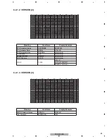
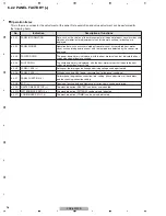
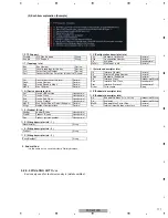
Cause of shut-down (MAIN)
Cause of shut-down (SUB)
Item
OSD Indication
Item
OSD Indication
Communication Error
RTRY
SQ-NON
BUSY
VER-HS, VER-MS
Drive Stop
Communication Busy
Drive Processing IC
SQ_LSI
Version mismatching (H/S) (M/S)
MAIN EEPROM Communication Error
EEPROM
BACKUP EEPROM Communication Error
BACKUP
MDU-IIC
MD-IIC
DAC1 Communication Error
DAC1
DAC2 Communication Error
DAC2
−
−
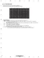
Panel temperature
Abnormally in RST2 power supply
TMP-NG
RST2
Low temperature of the panel
TEMP-L
High temperature of the panel
TEMP-H
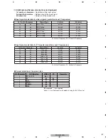
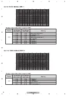
<Cause of shut-down and corresponding OSD Indication >
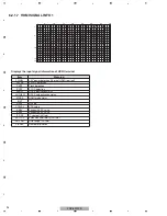
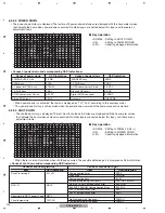
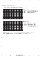
6.2.2.3 POWER DOWN
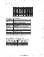
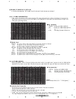
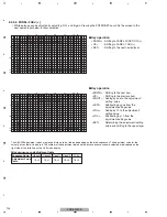
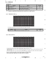
6.2.2.4 SHUT DOWN
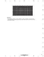
• The power-down history is displayed. The last most 8 power-down histories are displayed with the hour-meter values
that indicate the hours when power-downs occurred. No other layers are nested below this layer, and there are no
adjustment items.
• The shutdown history is displayed. The last most 8 shutdown histories are displayed with the hour-meter values
that indicate the hours when shutdowns occurred. No other layers are nested below this layer, and there are no
adjustment items.
<DOWN> : Shifting to SHUT DOWN
<UP>
: Shifting to PANEL WORKS
<L/R>
: Updating displayed information
g
Key operation
<DOWN> : Shifting to PANEL-1 ADJ (+)
<UP>
: Shifting to POWER DOWN
<L/R>
: Updating displayed information
g
Key operation
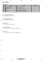
<Causes of power-down and corresponding OSD indications>
Cause of power-down
OSD Indication
Cause of power-down
OSD Indication
POWER SUPPLY Unit
P-PWR
X DRIVE Assy
XDRV
SCAN Assy
SCAN
DC/DC converter for X drive
X-DCDC
5 V power for SCAN Assy
SCAN5V
Y-DRV
X-drive SUS circuit
X-SUS
Y DRIVE Assy
DC/DC converter for Y drive
Y-DCDC
Y-drive SUS circuit
Y-SUS
Digital DC/DC converter
D-DCDC
Unknown
UNKNOWN
ADDRESS Assy
ADRS
*
When power-down is confirmed, the factor is displayed as "1st", "2nd", according to the accuracy order.
*
The power-down history is not recorded when the power-down occurred at the same place and same time.
*
When there is detail information when shutdown occurred, the possible defective part is displayed as Sub information.
1
5
10
15
16
1
5
10
15
20
25
30
32
1
2
3
4
5
6
7
8
9
A
B
C
D
E
A
.
P
N E L
O
P
W E R
O
D
W
S
1
T
N
2
D
N
3
8
2
0
0
0
1
– – –
–
–
2
Y – S
S
U
X – D
V
R
S C A
–
–
–
N
3
S C A N
– – – –
4
5
7
P O W
R
E
S C A N
– – –
–
D
–
–
C
–
–
X – D C
– – – –
8
6
S C A N 5 V
Y – D C
C
D
A D R S
H
0 4 M
1
7
7
0
0
0
H
1 6 M
0
1
4
0
0
0
H
4 4 M
0
1
4
0
0
0
H
3 2 M
0
1
4
0
0
0
H
2 9 M
0
3
1
0
0
0
H
4 2 M
0
2
1
0
0
0
H
1 1 M
0
0
0
0
0
0
H
5 1 M
H
M
F A C T
V
–
D 1
1
5
0 6 0
– N T V
T
A
–
B
1
5
10
15
16
1
5
10
15
20
25
30
32
1
2
3
4
5
6
7
8
9
A
B
C
D
E
A
.
N E L
H
P
S
U T
O
D
W
A
M
I N
U
S
B
N
3
8
2
0
0
0
1
T E M
–
P
H
2
S Q –
S
L
I
S Q –
T M
–
P
N G
B U S
H S
Y
3
M D – I I C
D A C 1
4
5
7
S Q –
S I
L
S I
L
V E R –
B U S Y
B A C K U P
8
6
M D – I I C
H
0 4 M
1
7
7
0
0
0
H
1 6 M
0
1
4
0
0
0
H
4 4 M
0
1
4
0
0
0
H
3 2 M
0
1
4
0
0
0
H
2 9 M
0
3
1
0
0
0
0
2
1
0
0
0
H
4 2
1 1
M
H
M
H
M
H
M
F A C T
V
–
D 1
1
5
0 6 0
– N T V
T
A
–
B
Summary of Contents for PDP-5010FD
Page 19: ...PDP 5010FD 19 5 6 7 8 5 6 7 8 C D F A B E ...
Page 20: ...PDP 5010FD 20 1 2 3 4 1 2 3 4 C D F A B E 4 BLOCK DIAGRAM 4 1 OVERALL WIRING DIAGRAM 1 2 ...
Page 23: ...PDP 5010FD 23 5 6 7 8 5 6 7 8 C D F A B E ...
Page 35: ...PDP 5010FD 35 5 6 7 8 5 6 7 8 C D F A B E ...
Page 167: ...PDP 5010FD 167 5 6 7 8 5 6 7 8 C D F A B E ...
Page 178: ...PDP 5010FD 178 1 2 3 4 1 2 3 4 C D F A B E 10 6 PANEL CHASSIS SECTION ...


