background image

PDP-5010FD

98

1

2

3

4

1

2

3

4

C

D

F

A

B

E

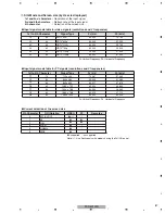
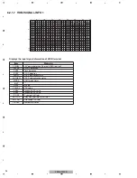
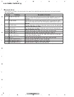
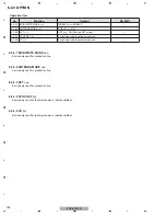
6.2.2  PANEL FACTORY (+)

This is the menu screen for the adjustment of the panel. Data acquisition and value adjustment can be performed for
the following items:

No.

Indication

Description of functions

6.2.2.1

PANEL INFORMATION

Data, such as the version of the microcomputer of the panel, product serial number, and 
statuses of memories for adjustment values for the main unit and for backup, are 
displayed.

6.2.2.2

PANEL WORKS

Operation data, such as accumulated pulse-meter count, accumulated hour-meter 
count, accumulated power-on count, and the temperature detected by the sensor, are 
displayed.

6.2.2.3

POWER DOWN

The power-down history is displayed, with the hour-meter values that indicate the hour 
values when power-downs occurred.

6.2.2.4

SHUT DOWN

The shutdown history is displayed, with the hour-meter values that indicate the hour 
values when shutdowns occurred.

6.2.2.5

PANEL-1 ADJ (+)

Settings of the driving pulse timing and driving voltage can be performed.

6.2.2.6

PANEL-2 ADJ (+)

White balance and ABL (power consumption) for the panel can be set.

6.2.2.7

PANEL FUNCTION (+)

Perform panel-degradation correction-level setting, phase adjustment of the address, 
and the streaking-correction setting.

6.2.2.8

ETC. (+)

Copying of backup data and clearance of various data can be performed.

6.2.2.9

RASTER MASK SETUP (+)

The mask indication (RASTER) can be set and indicated.

6.2.2.10 PATTERN MASK SETUP (+)

The mask indication (PATTERN) can be set and indicated.

6.2.2.11 COMBI MASK SETUP (+)

The mask indication (COMBI) can be set and indicated.

    Operation Items 

Summary of Contents for PDP-5010FD

Page 1: ...lgium PIONEER ELECTRONICS ASIACENTRE PTE LTD 253 Alexandra Road 04 01 Singapore 159936 PIONEER CORPORATION 2007 PDP 5010FD ARP3455 PLASMA DISPLAY SYSTEM PDP 5010FD THIS MANUAL IS APPLICABLE TO THE FOLLOWING MODEL S AND TYPE S Model Type Power Requirement Remarks PDP 5010FD KUCXC AC 120 V PDP 5010FD KUC AC 120 V For details refer to Important Check Points for good servicing T IZS 001 JULY 2007 Prin...

Page 2: ...be put back in place such as barriers nonmetallic knobs adjustment and compartment covershields isolation resistor capacitor etc 3 When service is required observe the original lead dress Extra precaution should be taken to assure correct lead dress in the high voltage circuitry area 4 Always use the manufacture s replacement components Especially critical components as indicated on the circuit di...

Page 3: ... not exceed 1 mA ANY MEASUREMENTS NOT WITHIN THE LIMITS OUTLINED ABOVE ARE INDICATIVE OF A POTENTIAL SHOCK HAZARD AND MUST BE CORRECTED BEFORE RETURNING THE SET TO THE CUSTOMER PRODUCT SAFETY NOTICE Many electrical and mechanical parts in PIONEER set have special safety related characteristics These are often not evident from visual inspection nor the protection afforded by them necessarily can be...

Page 4: ... the product Please check that neither solder debris nor screws remain inside the product 8 There should be no semi broken wires scratches melting etc on the coating of the power cord Damaged power cords may lead to fire accidents so please be sure that there are no damages If you find a damaged power cord please exchange it with a suitable one 9 There should be no spark traces or similar marks on...

Page 5: ...OCK of MAIN ASSY 36 4 13 TANSHI ASSY 38 4 14 50FHD LED and FHD IR ASSYS 39 4 15 POWER SUPPLY BLOCK of FHD RLS and SIDE KEY ASSYS 40 5 DIAGNOSIS 41 5 1 POWER SUPPLY OPERATION 41 5 1 1 LED DISPLAY INFORMATION 41 5 1 2 POWER ON SEQUENCE 42 5 1 3 DETAILS OF POWER ON SEQUENCE 43 5 2 DIAGNOSIS FLOWCHART OF FAILURE ANALYSIS 45 5 2 1 WHOLE UNIT 45 5 2 2 POWER SUPPLY UNIT 47 5 2 3 DRIVE ASSY 48 5 2 4 DIGIT...

Page 6: ...ARE REPLACED 141 8 6 PRECAUTION ON REPLACEMENT OF THE POWER SUPPLY UNIT 144 9 RS 232C 145 9 1 OUTLINE OF RS 232C COMMAND 145 9 1 1 PREPARED TOOLS 145 9 1 2 USING RS 232C COMMANDS 145 9 2 LIST OF RS 232C COMMANDS 146 9 3 DETAILS OF EACH COMMANDS 155 9 3 1 QS1 PANEL STATUS 155 9 3 2 QS2 PANEL OPERATION DATA 156 9 3 3 QS3 OTHER DATA ON THE PANEL 157 9 3 4 QAJ PANEL ADJUSTMENT DATA 158 9 3 5 QPW VIDEO...

Page 7: ... higher melting points by approximately 40 C Therefore for lead free soldering the tip temperature of a soldering iron must be set to around 373 C in general although the temperature depends on the heat capacity of the PC board on which reworking is required and the weight of the tip of the soldering iron Compared with eutectic solders lead free solders have higher bond strengths but slower wettin...

Page 8: ... 270 V to 400 V 50F SCAN C Assy 270 V to 400 V 50F SCAN D Assy 270 V to 400 V Part is the High Voltage Generating Points other than the Charged Section High Voltage Generating Point 50F Y DRIVE Assy POWER SUPPLY Unit 50F X DRIVE Assy Conductive plate X 50F SCAN D Assy 50F SCAN C Assy 50F SCAN B Assy 50F SCAN A Assy Charged Section The places where the commercial AC power is used without passing th...

Page 9: ... 2 SXG1127 Bracket Assy C SXG1128 Speaker mounting screw M5 x 10 mm Black 9 BMZ50P100FTB Power cord 2 m 6 6 feet ADG1215 Alkaline dry cell battery LR6 AA Binder Assy AEC1908 Cleaning cloth AED1285 Warranty card Operating instructions PDP 5010FD KUCXC ARE1472 Operating instructions PDP 5010FD KUC ARE1487 Speed clamp 3 Screw 2 M4 10 mm for plastic bands Plastic band 2 Bead band 3 Speaker accessories...

Page 10: ...signal detection PLL full synchronous detection PLL digital Synthesizer system VHF Ch 2 to 13 UHF Ch 14 to 69 VHF UHF Tuner CATV VHF UHF Tuner BTSC system Terminals Rear 75 Ω UNBAL F Type for DTV VHF UHF CATV in ANT CABLE A IN Ch 1 to 135 ANT B IN Ch 1 to 125 75 Ω UNBAL F Type for VHF UHF CATV in S VIDEO in VIDEO in AUDIO in COMPONENT VIDEO in VIDEO in AUDIO in HDMI in AUDIO in HDMI in AUDIO in HD...

Page 11: ...Y ON on the plasma display is pressed To turn on the power press 2 POWER ON indicator 3 STANDBY indicator 4 SLEEP indicator 5 Room Light Sensor 6 Remote control sensor 7 STANDBY ON button1 8 INPUT button ENTER button 9 VOLUME UP DOWN buttons UP DOWN buttons 10 CHANNEL UP DOWN buttons LEFT RIGHT buttons 11 TV GUIDE button 12 USB port 13 PHONES output terminal 14 INPUT 3 terminals COMPONENT VIDEO Y ...

Page 12: ...8 INPUT 7 terminal HDMI 9 PC INPUT terminal ANALOG RGB 10 CONTROL OUT terminal 11 RS 232C terminal used for factory setup 12 ANT B IN terminal 13 INPUT 1 terminal S VIDEO 14 INPUT 1 terminal VIDEO 15 SUB WOOFER terminal 16 AUDIO OUT terminals AUDIO 17 INPUT 1 terminals AUDIO 18 INPUT 2 terminals AUDIO 19 INPUT 4 terminals AUDIO 20 INPUT 5 terminals AUDIO 21 INPUT 2 terminal VIDEO 22 DIGITAL OUT te...

Page 13: ... Displays the HDMI Control menu 11 FAVORITE CH A B C D Selects any of the four preset channels While watching you can toggle the set channels by pressing A B C and D 12 0 to 9 Selects the channel 13 dot Enters a dot 14 CH Selects the channel 15 SPLIT Switches the screen mode among 2 screen picture in picture and single screen 16 FREEZE Freezes a frame from a moving image Press again to cancel the ...

Page 14: ...d interrupted Mottled color No Procedures Item to be checked 1 Check if all the symptoms pointed out by the customer have been addressed The symptoms in question must not be reproduced 2 Connect the peripheral equipment Connect all external peripheral equipment as originally connected and check if the connections are correct 3 Check the video and audio Tune in to the stations that the customer wou...

Page 15: ...value 1 Select PANEL FACTORY ETC then P COUNT INFO After entering Factory mode press MUTING once press ENTER SET press j seven times press ENTER SET then press j six times 2 Press l to select CLEAR Hold ENTER SET pressed for at least 5 seconds After clearance is completed ETC is automatically selected Clear the maximum temperature value MAX TEMP in the same manner 4 Other Assys Clearance of the ma...

Page 16: ... 3 AFT 4 SYNC DET To shift to another mode press MUTING To shift to another item in a specific mode press i or j To shift to the next nested layer below for an item with a indication press ENTER SET To return to the next nested layer above also press ENTER SET Mode transition in Service Factory mode Up Down Structure of Layers in Panel Factory Mode 2 7 PANEL FUNCTION 1 R LEVEL 2 G LEVEL 3 B LEVEL ...

Page 17: ...AWW1311 NSP 50F SCAN A ASSY AWW1312 IC2801 IC2804 AN16174A NSP 50F SCAN B ASSY AWW1313 IC2901 IC2904 AN16174A NSP 50F SCAN C ASSY AWW1314 IC3001 IC3004 AN16174A NSP 50F SCAN D ASSY AWW1315 IC3101 IC3104 AN16174A 50F X DRIVE ASSY AWV2510 50F Y DRIVE ASSY AWV2511 PANEL SENSOR ASSY AWW1309 50F DIGITAL ASSY AWW1316 Mark No Description Part No MAIN ASSY AWV2457 SIDE IO ASSY AWW1274 SIDE KEY ASSY AWW127...

Page 18: ...ST 3 5 CLEANING Service Cotton Cloth Glove GYX1002 7 3 DISASSEMBLY AND REASSEMBLY PRECAUTIONS FOR SPEAKER SYSTEM Name Jig No Remarks Name Part No Remarks Cleaning liquid GEM1004 Used to fan cleaning Refer to 10 4 CHASSIS SECTION 1 2 Cleaning paper GED 008 ...

Page 19: ...PDP 5010FD 19 5 6 7 8 5 6 7 8 C D F A B E ...

Page 20: ...PDP 5010FD 20 1 2 3 4 1 2 3 4 C D F A B E 4 BLOCK DIAGRAM 4 1 OVERALL WIRING DIAGRAM 1 2 ...

Page 21: ...ing service parts be sure to refer to EXPLODED VIEWS and PARTS LIST or PCB PARTS LIST The mark found on some component parts indicates the importance of the safety factor of the part Therefore when replacing be sure to use parts of identical designation ...

Page 22: ...PDP 5010FD 22 1 2 3 4 1 2 3 4 C D F A B E 4 2 OVERALL WIRING DIAGRAM 2 2 V 8V_AU V 3_3V_A V 3_3V_AU_D ...

Page 23: ...PDP 5010FD 23 5 6 7 8 5 6 7 8 C D F A B E ...

Page 24: ...IC1601 LVDS Receiver AN P BN P CN P DN P CLKN P AD1 CN1602 AD2 CN1601 50F ADDRESS L ASSY DRIVER IC IC1661 DRIVER IC IC1671 DRIVER IC IC1681 CLK LE HBLK LBLK R G B DRIVER IC IC1651 VDDLS4 VADR4 VADR3 VDDLS3 VADR2 VADR1 VDDLS2 VDDLS1 RESONANCE BLOCK RESONANCE BLOCK RESONANCE BLOCK RESONANCE BLOCK V 60V V 8V V 3 3V IC1601 LVDS Receiver AN P BN P CN P DN P CLKN P AD1 CN1602 AD2 CN1601 50F ADDRESS S AS...

Page 25: ... AD1 CN1602 AD2 CN1601 50F ADDRESS L ASSY CLK LE HBLK LBLK R G B DRIVER IC IC1651 DRIVER IC IC1661 DRIVER IC IC1671 DRIVER IC IC1681 VDDLS4 VADR4 VADR3 VDDLS3 VADR2 VADR1 VDDLS2 VDDLS1 RESONANCE BLOCK RESONANCE BLOCK RESONANCE BLOCK RESONANCE BLOCK V 60V V 8V V 3 3V IC1601 LVDS Receiver AN P BN P CN P DN P CLKN P AD1 CN1602 AD2 CN1601 50F ADDRESS L ASSY CLK LE HBLK LBLK R G B DRIVER IC IC1651 DRIV...

Page 26: ... GY_VDEC VBI_Y V L R L R Input 4 HDMI Input 5 HDMI Input2_Y Pb Pr L R TANSHI ASSY MAIN ASSY V MAP5601M MAP Input 3 IC4701 R2S11001FT RGBSW DA_RCR DA_BCB DA_GY SDA_AV5 SCL_AV5 CLP_RGB Input3_Y Pb Pr SIDE IO ASSY PC_RGB PC_H V PC Input SDA_AV SCL_AV I2S_BCLK_DTV I2S_LRCLK_DTV I2S_SDATA_DTV SPDIF_DTV I2S_BCLK_HDMI I2S_LRCLK_HDMI I2S_SDATA_HDMI SPDIF_HDMI IC8301 AGC1037 RS232C TXD RXD SR_OUT RXD_SR TX...

Page 27: ...N6_GY DIN1_DVO EXT_HD1 VD1 RST_ASIC RXD_IC3 TXD_IC3 AGC1049 16Mbit Flash VD1 HD1 VD7 HD7 TXD_MD RXD_MD REQ_MD VD7_0 HD7_0 IC8401 UPD61123F1 IC5201 SII9025CTU HDMI RX LED_ON1 ON2 OFF EMMA2SV RST3 IC5101 CXB1442 DSCL_1 DSDA_1 Input 5 HDMI Input 4 HDMI IC8402 AGC1039 FLASH IC4310 PQ200WNA1ZPH FAN CONTROL IC4303 PQ200WNA1ZPH FAN CONTROL Input 6 HDMI Input 7 HDMI HDMI SW TRAP SW LED TRAP SW 50 FHD LED ...

Page 28: ...V D109 D108 T701 T501 T101 P3 P1 P2 P7 P6 P5 P8 16 5V 6 5V VSUS_ADJ Q702 Q701 Switching Switching P4 5 1V T402 5 1V P9 Switching IC101 P12 STB5 1V STB3 3V STB3 3V 12V STB5 1V P11 P10 16 5V 6 5V 12V 16 5V 16 5V 6 5V 35V 16 5V 12V F101 D106 DRF_SW_B AC_DET M_SW_DET PD_TRIG_B DRF_B US_SW Q203 Q902 Q901 Q502 Q501 Switching Switching Switching Switching 12V 12V T401 5 1V 5 1V AC_DET M_SW_DET IC202 AC_D...

Page 29: ...gnal Drive Signal RESONANCE BLOCK PSUS 5V OFFSET Reg Drive Signal SUS PreDrive PU 16 5V VSUS SUS BLOCK VSUS SUS BLOCK SOFT D 16 5 XPRST 16 5 VSUS 16 5V PSUS LOGIC BLOCK 16 5V 15V DC DC CONV VPU VPOFS REGULATOR REGULATOR 12V 5 1V 8V 3 3V X 7 60V 12V 5 1V 16 5V 5V VSUS 6 5V X 2 REGULATOR X 6 60V 8V 3 3V VSUS SUS BLOCK X 5 60V 8V 3 3V X 4 3 3V 8V 60V X 3 3 3V 8V 60V ...

Page 30: ...V VH IC5V SB2 PSUS Scan Signal Scan Signal VH IC5V SC2 Scan Signal VH IC5V Y 1 Y 3 PSUS PSUS Scan Signal IC5V Y 5 Y 9 Y 8 16 5V IC5V VF DC DC CONV IC5V VC_P 16 5V 15V DC DC CONV VC_S VC_U 5V LOGIC BLOCK Drive Signal VSUS VYPRST VSNOFS VKNOFS2 VKNOFS3 VKNOFS4 VKNOFS1 MAIN DC DC CONV VH VH IC5V Y 2 Photo Coupler BLOCK Y 4 VSUS SUS BLOCK VSUS SUS BLOCK VSUS SUS BLOCK SUS PreDrive 16 5V VC_S H MSK VC_...

Page 31: ...C5V Scan Logic Scan IC 15V HMSK FET Pre drive Logic 5V DC DC Conv SUS G FET Pre drive SUS B FET Pre drive SUS U IGBT Pre drive SUS D IGBT Pre drive XPRST FET Pre drive XSOFT G FET Pre drive XKOFS1 FET Pre drive XKOFS2 FET Pre drive VXKOFS1 Reg VXKOFS2 Reg Logic SUS G FET Pre drive SUS B FET Pre drive SUS U IGBT Pre drive SUS D IGBT Pre drive LMSK FET Pre drive YPRST FET Pre drive SNOFS FET Pre dri...

Page 32: ...IVER IC IC1871 DRIVER IC IC1851 DRIVER IC IC1651 VDDLS4 VADR4 VADR3 VDDLS3 VADR2 VADR1 VDDLS2 VDDLS1 VADR3 VDDLS3 VADR2 VADR1 VDDLS2 VDDLS1 RESONANCE BLOCK RESONANCE BLOCK RESONANCE BLOCK RESONANCE BLOCK RESONANCE BLOCK RESONANCE BLOCK RESONANCE BLOCK V 60V V 8V V 3 3V V 60V V 8V V 3 3V IC1601 LVDS Receiver IC1801 LVDS Receiver AN P BN P CN P DN P CLKN P AN P BN P CN P DN P CLKN P AD1 CN1602 AD1 C...

Page 33: ...ELAY V 1_1V_D V 1_8V_D V 3_3V_D RESETX AND V 1_1V_D V 2_5V_D LVDS 1 2V REG V 2_5V_D V 1_2V_D 1 8V REG V 2_5V_D V 1_8V_D D23 D24 SCL SDA TEMP1 D21 D16 D15 D14 D13 STOP_SQ VH_UV_PD YDRIVE_PD YRESNC_PD YDD_CHV_PD IC5V_UV_PD VOFS_ADJ YPRST_ADJ XKNOFS1_2_ADJ XKNOFS3_ADJ XKNOFS4_ADJ SCL SDA SCL SDA Flash Memory IC3302 UART LVDS Reciever IC3201 LVDS Reciever IC3202 V 3VACTV D11 SUB FILD CONV XY DRV SEQUE...

Page 34: ...SAW filter RF AGC To TANSHI ASSY CN4001 SDRAM IC6603 256Mbit SDRAM IC6604 256Mbit SDRAM IC6605 256Mbit QPSK IF Down Conv IC6201 IF SW IC6103 EEPROM 64Kbit IF HSX_0 I2C_TUNER_SCL I2C_TUNER_SDA Logic Circuit DVO 12bit OOB_Data TS0 I2C0 EBI BUS MEMORY BUS UARTA From EMMA2 To ARIA To AV_SW I2C SW IC6102 SCL_AV5 SDA_AV5 From VDEC YUV 656 8bit To POD ASSY CN4005 CN4006 FLASH 32M IC6902 VBI SLICER IC7001...

Page 35: ...PDP 5010FD 35 5 6 7 8 5 6 7 8 C D F A B E ...

Page 36: ...for Main BoardFAN for EMMA for IF U COM for AV_SW RGB_SW HDMIROM 7038EEPROM 7038IIC A D for USB DLNA IC6402 Switch IC V 5V_USB R5523H001B Filter V 3_3V_UCOM for EMMA for EMMA IC4301 8V LEG Variable REG V 8V_AIR AU A A2 DSP PQ200WNA1ZPH for POD VPP for POD_VCC Discrete 30V REG V 30V_ANT_A Discrete 30V REG V 30V_ANT_B IC4404 DD com V 1_2V_D LTC3416 for 7038 3517 IC4501 DD com DD com V 2_5V_UCOM LTC3...

Page 37: ..._UCOM_VBI IC4403 3ch DD com V 2_5V_D BD8602FV 3 SP8M4 Q4411 FET Switch V 2_5V_D2 RSS100N03 IC4403 3ch DD com V 1_2V_D2 BD8602FV 3 RSS100N03 RSS090P03 3ch DD com BD8602F V for 7038 3517 ARIA VBI Q4415 FET Switch V 3_3V_D2 RTQ040P02 for VDEC_D HDMI HDMI_SW IC4403 3ch DD com V 3_3V_D BD8602FV 1 SP8M4 for 7038 3517 POD DT_D DSP ARIA LVDS VDEC_D ADC HDMI HDMI_SW VBI Q4404 FET Switch V 3_3V_D4 RTQ040P02...

Page 38: ...IC9181 NJM78M12DL1A 1 8V 16 5V 16 5V 12V INPUT AUDIO 16 5V SCL_AV REGULATOR IC9191 NJM2846DL3 3 3V 1 8V 3 3V IO3 RST_MSP I2S_DTV SPDIF_HDMI IO5 3 3V 8V OUTPUT AUDIO SPDIF_DTV OPT_OUT L OUT R OUT IO8 A_NG_B DC DETECT BLOCK R_OUT R_OUT L_OUT L_OUT OTW IO9 IO4 IO1 INPUT VIDEO AIR INPUT3 AUDIO CVBS HP IO2 INPUT3 YPbPr LPF SP TERMINAL OPTICAL OUT SUB WOOFER OUT AUDIO OUT INPUT1 INPUT2 INPUT3 INPUT4 INP...

Page 39: ...IR ASSYS FAN FAN FAN FA3 FA4 FA5 M5 FA1 FHD FAN CONNECT ASSY DIGITAL ASSY POWER SUPPLY UNIT D11 P8 P9 USB FAN LED_ON M1 M3 M2 M21 M4 LED_OFF M11 50FHD LED ASSY MAIN ASSY M15 M6 M8 M9 FHD IR ASSY FHD RLS ASSY IO4 IO3 IO5 IO_AUDIO ASSY M33 C1 M34 C2 POD ASSY LED_TIMER ...

Page 40: ... 1 2 3 4 C D F A B E 4 15 POWER SUPPLY BLOCK of FHD RLS and SIDE KEY ASSYS FHD RLS ASSY SIDE KEY ASSY MAIN ASSY CN9781 OP AMP IC9781 MM3012XN V 3_3V_UCOM RLS IC9782 AMS114YD01 CN9501 KEY S9501 to S9507 V 3_3V_STB MAIN ASSY ...

Page 41: ...e Red Orange Blue Red Orange Blue Red Orange Blue Red Orange Blue Red Orange Blue Red Orange Blue Red Orange Downloading of DTV Module software is abnormally finished Downloading of DTV Module software is finished normally Blue Red Orange Blue Red Orange Once Twice n times Lightins out Lightins out Lightins out Lightins out Lightins out Lightins out Lightins out Lightins out Lightins out Lightins ...

Page 42: ...ssues a startup command PON to the MOD microcomputer 4 The relay is controlled with logical OR interpretation of control signals by the main microcomputer and module MOD microcomputer MOD Microcomputer IC3151 MAIN Microcomputer IC8401 IF Microcomputer IC8301 Power MOD RELAY Control REM Inv Amp Q9731 REM infrared receiver Side Keys SR OUT Jack JA9404 4 1 2 1 SR_OUT KEY_1 KEY_2 TXD_MD RXD_MD REQ_MD ...

Page 43: ...V 5 1V VSUS VADR PDET AND Main Switch AC RST2 Jumper MOD_ RST RGB SW AD ON OFF AV SW FAN ASIC RST3 M_SW_DET_B M_SW_DET AC_DET P11 US_SW A TUNER D TUNER VBI BCM iLink AAC DEC GR USB MAP A D TUNER COFDEM CIF VDEC HDMI ASIC LVDS Tx EMG_USB MSP A D TUNER A TUNER VBI BCM POD USB Reg DLNA USB Elite MAP Main_ ucom OR LVDS Rx DAC SQ ASIC LED DCDC REG DCDC REG DRIVE SCAN IR Key 232C DCDC REG AND ADDRESS DR...

Page 44: ...V V 6 5V V 5 1V VSUS VADR PDET AND Main Switch AC RST2 Jumper MOD_ RST RGB SW AD AC_ DET ON OFF PON AV SW FAN ASIC RST3 M_SW_DET_B M_SW_DET AC_DET SW P11 US_SW A TUNER D TUNER VBI BCM iLink AAC DEC GR USB MAP A D TUNER COFDEM CIF VDEC HDMI ASIC LVDS Tx EMG_USB MSP A D TUNER A TUNER VBI BCM POD USB Reg DLNA USB Elite MAP IF ACTIVE Main PSW1 Module RELAY Module DRF_B Main RST4 Main RST2 Module RST2 ...

Page 45: ...e RELAY port of the connectors between the DIGITAL Assy and POWER SUPPLY Unit H 3 3 V No No Is the drive off Turn the drive on Is the abnormality associated with a single scan line No Yes Yes Yes Yes A power down occurs Does the screen display reset lighting Is there any local abnormality on the screen Is the abnormality associated with one ADDRESS or one TCP See 5 3 DIAGNOSE OF PD POWER DOWN Yes ...

Page 46: ...ge No No Failure analysis for the audio system AU1 Yes Yes Yes In the subsequent diagnostic steps it is most likely that the multi base section is in failure Problems concerning video display Problems concerning the audio output A Failure analysis for the DIGITAL Assy DG1 Failure analysis for the MAIN Assy MA3 A main microcomputer may stop in the state that it hung a panel mute due to something Is...

Page 47: ...s normal STB 3 3 V power is not output No Is the VADR voltage within the specified values Is the VSUS voltage within the specified range Is there a fluctuation in the VADR voltage Is there a fluctuation in the VSUS voltage The ripple must be within 5 V The ripple must be within 10 V The specified voltage values are between 57 and 63 V The specified voltage values are between 200 and 210 V VSU 125 ...

Page 48: ...ys connectors properly connected to the X Y DRIVE Assys Is the input signal normal Replace the panel chassis Yes Replace the X Y DRIVE Assys NG Replace the DIGITAL Assy Properly connect the panel FPC and SCAN Assys connectors Properly connect the FFC cables No Replace the FFC cables Reset lighting is not displayed Is the waveform normal when the voltage is applied to the panel Failure analysis for...

Page 49: ...lace the FFC cables Replace the DIGITAL Assy Replace the Y DRIVE Assy Replace the SCAN IC NG NG Yes Yes Yes Yes No Set the VYRST voltage correctly Is the VYRST set voltage correctly set set value designated for each panel NG Yes No Set the VKNOFS1 2 voltage correctly Is the VKNOFS1 2 set voltage correctly set NG NG Yes Yes No Set the VKNOFS3 voltage correctly Is the VKNOFS3 set voltage correctly s...

Page 50: ...s Is the VXKOFS2 set voltage correctly set Yes Another Assy may be in failure X DRIVE Assy No Replace the FFC cables Replace the DIGITAL Assy Replace the X DRIVE Assy NG NG Yes Yes Is the input signal normal See the oscilloscope photos No Are all the connectors properly connected Reconnect the connectors No C NG Yes Is the TCP control signal normal See the oscilloscope photos Yes ADDRESS Assy Repl...

Page 51: ...is in failure the abnormality is associated with one address in most cases Replace the panel chassis No NG Yes Yes Yes No Is the Three pieces connector connected properly to the socket Reconnect the connector properly NG Is the waveform of the SCAN IC control signal from the Y DRIVE Assy normal No Replace the Y DRIVE Assy The abnormality is associated with a single scan line Diagnose the SCAN A B ...

Page 52: ...AL Assy which can easily be damaged If the OSD is not properly displayed although the panel mask is properly displayed a failure exists in the path from the output of IC2801 on the MAIN Assy to IC3301 on the DIGITAL Assy If only the OSD is abnormal the MAIN Assy is in failure In a case of D11 It is most likely that the sync signal is abnormal It is most likely that the video signal data are missin...

Page 53: ... Failure in the line between the IF microcomputer and M11 connector Failure in the RS 232C driver and its peripheral circuits Failure in the Main microcomputer No Replace the MAIN Assy Yes Is the voltage at Pin 3 of the M11 connector High Relay control is unable unless it supplies a power supply to the module microcompute No Replace the MAIN Assy No Turn the POWER switch on Does the POWER switch o...

Page 54: ...the HDMI SIGNAL INFO data again NG Replace the MAIN Assy No Replace the MAIN Assy The input signal is not displayed TV Is the selected input signal a composite signal Yes No COMP S PC Is the selected input signal a component signal Yes COMP PC1 Is the selected input signal a S video signal Is the selected input signal an PC signal Yes No Is the selected input signal an HDMI signal Yes Yes DTV Is t...

Page 55: ...video signal is not displayed COMP S Is the compornent cable is connect to jack Input1 to Input3 Has the signal arrived at IC4601 pins 85 91 72 Yes Which signal is not output main or sub signal Is a signal output from IC4601 pins 42 45 Yes Has the signal arrived at IC4801 pins 22 26 Yes Has the symptom been settled when the MAIN Assy is replaced Yes Yes Is the communication between each IC on the ...

Page 56: ...IC4601 pins 55 57 Yes Which signal is not output main or sub signal Is a signal output from IC4601 pins 42 45 Has the signal arrived at IC4801 pins 22 26 Yes Has the symptom been settled when the MAIN Assy is replaced Yes Yes Is the communication between each IC on the MAIN Assy and the microcomputer normal Yes Has the signal arrived at IC4801 pin 70 Yes MAIN SUB 2 4 8 Is a signal output from IC46...

Page 57: ...he signal arrived at IC4701 Yes Is a signal output from IC4701 pins 30 32 34 Has the signal arrived at IC5001 pins 43 48 54 Yes Has the symptom been settled when the MAIN Assy is replaced Yes Yes Is the communication between each IC on the MAIN Assy and the microcomputer nomal Yes 15 18 14 13 17 16 13 IC4701 pin 30 component_PR V 500 mV div H 10 μsec div 13 IC4701 pin 30 PC_R V 500 mV div H 10 μse...

Page 58: ...in 43 48 54 Yes Has the symptom been settled when the MAIN Assy is replaced Yes Yes Is the communication between each IC on the MAIN Assy and the microcomputer nomal Yes 15 18 14 13 12 11 10 17 16 13 IC4701 pin 30 component_PR V 500 mV div H 10 μsec div 13 IC4701 pin 30 PC_R V 500 mV div H 10 μsec div 15 IC4701 pin 34 component_Y V 500 mV div H 10 μsec div 15 IC4701 pin 34 PC_G V 500 mV div H 10 μ...

Page 59: ... DTV Digital Terrestrial Video is not displayed DTV Finishing troubleshooting Has the function is selected Home Media Gallery by Home menu Select the input of specification by the input switch Has USB memory or digital camerra is connected to USB connecter No Insert USB device such as USB flash memory NG NG No Check between IC6401 and IC8001 If there is no problem then replace IC6401 No The panel ...

Page 60: ...air the failure points Is a 12 V output from 12V_Reg output of IC9181 normal Yes Check the peripheral circuits and the communication with the microcomputer and clock output of X9101 If there was no ploblem replace the MAP5601M Are signals input to IC9151 pins 2 3 5 6 Yes Check the IC9151 and peripheral circuit Repair the failure points Are signals output from IC9151 pins 1 7 No Check between the L...

Page 61: ...pins 1 7 Yes Replace the cables or SIDE IO Assy NG Check the cables between CN8801 and CN9351 or check around the Headphones jack B 42 43 47 48 Waveforms Input signal L R 1 kHz 0 5 Vrms VOL 30 44 49 45 50 46 51 52 53 CN9251 pins 2 4 V 2 V div H 1 mS div IC9101 pins 54 55 V 2 V div H 5 μS div CN9251 pins 5 7 V 2 V div H 1 mS div IC9101 pins 24 25 V 2 V div H 1 mS div 52 53 IC9101 pins 38 39 V 1 V d...

Page 62: ...signal input to IC9101 pins 100 to 102 Yes Is a SPDIF signal input to IC9101 pin 4 Check the communications around the IC9101 and between the IC9101 and the microcomputer If there was no ploblem replace the MAIN Assy Is a signal output from IC8401 of the MAIN Assy No Repare the DTB block Check around IC8401 and repair the failure points Check between input terminal and IC9101 and repair the failur...

Page 63: ... Protection Circuit Module Microcomputer PD MUTE Circuit YSUS_PD YDD_PD YDRV_PD SCN5V_PD SCAN_PD XDRV_PD XDD_PD XSUS_PD ADR_PD1 DIGI_DCDC_PD DRF_SW DRF_SW PD_MUTE_B PS_PD EXT_PD PD_TRIG_B D23 IC3604 12 IC3801 DCDC Converter IC3601 D3601 to D3605 D3608 D3612 D3501 to D3504 D13 to D20 D22 D21 Y1 Y1 X1 AD1 AD1 Note The figures to indicate the number of times the LED flashes when power down occurs in ...

Page 64: ...LOCK LMSK is short circuited VKOFS3 Regulator Q2706 Q2703 VKOFS4 UVP Y MSK BLOCK LMSK is short circuited EXT_PD line Open EXT_PD line Open It becomes UNKNOW except above mentioned PD detection condition VKOFS4 Regulator Q2707 Q2704 7 Y SUS Y DRIVE Assy Center electric potential detection PD Y RESONANCE BLOCK Q2106 to Q2109 Q2111 Q2113 D2104 to D2107 8 ADRS ADDRESS Assy ADDRESS RESONACE BLOCK VADR ...

Page 65: ...N1202 POWER SUPPLY Unit ADR system power 8 ADRS CN1203 ADDRESS Assy 8 ADRS Y DRIVE Assy CN2001 DIGITAL Assy 3 SCAN CN2301 POWER SUPPLY Unit drive system power 3 SCAN CN2302 POWER SUPPLY Unit ADR system power 8 ADR CN2303 to CN2306 ADDRESS Assy 8 ADR CN2501 CN2502 CN2801 CN2902 CN3002 CN3101 SCAN A B C D Assy SCAN A B C D Assy 4 SCN 5V SCAN A B C D Assy CN2901 CN3001 Y DRIVE Assy 4 SCN 5V ADDRESS A...

Page 66: ...tection Increase or decrease voltage detection Decrease voltage detection DCDC converter drive stop Increase or decrease voltage detection Resonance center electric potential 2 Increase or decrease voltage detection Increase or decrease voltage detection FFC disconnection detection YDRV_PD VXKOFS1 Decrease voltage detection VXKOFS2 Decrease voltage detection 15VDD Decrease voltage detection VPRST ...

Page 67: ...AV SCL_AV5 SDA_AV5 SCL_MA SDA_M IC5001 ADC IC5201 HDMI_RX IC8404 EEPROM U6001 A FE IC4601 AV SW IC4701 RGB SW SCL_MB SDA_M IC8301 IF_UCOM MODULE _UCOM EMMA2_UCOM OTW ANT_POW_DE V 12V V 6_5V V 5_1V IC4403 3chDC EMG_DDC IC8406 AND Gate IC8406 AND Gate V 3_3V_D4 EMG_USB IC6001 MPX U6101 AD FE IC6301 BCM3517 IC6401 BCM7038 TXD_DT RXD_DT IC7302 POD Interface IC6903 EEPROM IC7001 TV G slicer FAN NG2 M5 ...

Page 68: ...s in contact with the chassis AUDIO_AMP IC9201 IC9101 Check if the AMP output is short circuited Periphery of the cable between IO3 and M8 and IO6 and P5 CN8803 CN4001 CN8806 P5 Check if cables are firmly connected Blue 6 Failure in communication with the module microcomputer MODULE Communication line between MAIN and MOD IC3151 IC8401 Check the communication lines TXD_MOD RXD_MOD REQ_MOD Peripher...

Page 69: ...up error Blue 11 High temperature of the unit TEMP2 Temperature sensor or its periphery TEMP2 A shutdown occurs because of high temperature Periphery of the temperature sensor TH9091 TEMP2 Periphery of the cable between IO4 and M6 CN8804 CN4004 Check if cables are firmly connected Blue 12 Blue 15 Digital Tuner Main EEPROM DTUNER MA EEP Startup of BCM7038 IC6401 Check the startup of the BCM7038 and...

Page 70: ...r is possible but recording is not possible The video signal output from the DIGITAL connector is copy protected Miscellaneous The no signal off function is not activated The no signal off and no operation off functions are effective only if video composite S video component HDMI excluding PC input or TV input is selected The no operation off function is not activated Power management does not fun...

Page 71: ...gures in a case where an AV device such as an AV amplifier and a DVD recorder BD player are connected in a case where only a DVD recorder BD player is connected and in a case where an AV device such as an AV amplifier which does not support HDMI CEC is connected When an AV device that supports the HDMI Control function is connected it must be connected between the PDP and a DVD recorder BD player ...

Page 72: ...nstructions 1 Turn on the plasma television and all the connected devices 2 Confirm that the setting in Input Setting for HDMI Control Setting is properly entered according to the connected devices Also confirm the HDMI Control related settings in the connected devices 3 Switch to the HDMI input terminals to which the devices are connected to check if audio and video images are properly output and...

Page 73: ...asma discharge is about 700 it takes about 15 minutes to reach the lowest limit although the required time varies depending on the displayed picture The maximum count of plasma discharge will begin to increase gradually if the displayed picture is changed to animated picture Note How to decrease the brightness level in this function is the same as in high temperature protection function 1 Panel pr...

Page 74: ...ER SUPPLY Unit and GND Multi base section recommended using a jumper with alligator clips refer to the photos below 2 Execute DRV S00 by RS 232C command DRV S01 for release Supplemental explanation When the panel drive power is in OFF state there will be no PD except PS_PD as the PD signal has been muted If the clip is removed in the OFF state of the panel drive power PD will take place at the ins...

Page 75: ...decreases When the voltage of the DAC output for external FAN decreases rotation speed of FAN rises DIGITAL Assy TANSHI Assy If an emergency signal is detected it will be transmitted DAC output Block diagram Operation specifications Notes FAN_VCC1 0 to 12V 0 to 12V FAN_VCC2 TEMP2 FAN_NG1 FAN_ON1 FAN_CONT1 FAN_NG2 FAN_ON2 FAN_CONT2 HIGH LOW Temperature SD STOP 36 0 ºC 39 0 ºC 39 0 ºC 42 0 ºC 62 0 º...

Page 76: ... OTW MAIN Assy TANSHI Assy 1 When a shutdown decision is made by the main CPU After a warning indication is displayed for 5 sec a shutdown is generated the blue LED flashes 5 times A warning indication is displayed for all input signal types Example of a warning indication The speaker terminals are short circuited After reconnection turn the unit on again For 50 inch models For 42 inch models an i...

Page 77: ...gnal at the RST3 port continues to be H after 30 mS of waiting monitoring is continued If RST3 is L a restoration process starts according to the latest power on off status RST4 MAIN power RELAY Shutdown occurs if the signal is L for 5 sec after RELAY is ON or for 2 sec while the unit is ON or in Functional STB Functional STB Panel ON Areas other than North America While the main power switch is s...

Page 78: ...ic LED flash pattern blue LED 10 times starts The next PON operation is valid and the flag is cleared upon the next power on RST4 H Monitoring starts 1 sec after the above conditions are established If any values equal to or greater than minimum to require a shutdown are detected established under the monitoring conditions a warning indication will be displayed for 30 sec after which a shutdown pr...

Page 79: ...hen performing internal diagnosis of the PDP fix the switch to the OFF position using adhesive tape before turning on the unit After servicing be sure to remove the adhesive tape WHEN THE TRAP SWITCH IS ACTIVATED When the TRAP switch is activated the red and blue LEDs will light In order to deactivate the TRAP switch close the upper plate of the unit or fix the TRAP switch to the OFF position in t...

Page 80: ...nction is changed The signal mode is changed INFORMATION MTB INFORMATION How to enter Service Factory Mode By using a PDP service remote control PDP service remote control Press FACTORY key By issuing RS 232C commands During normal Standby mode Issue PON then FAY During normal operation mode Issue FAY How to exit Service Factory Mode By using a PDP service remote control PDP service remote control...

Page 81: ...unctions are set to OFF when Service Factory mode is entered including when the FAY command is received Note Enter the factory after cancelling ACI because the ACI operation setting OFF and not done Fuctions whose setting are set to OFF Function Remarks 2 Screen Operation Input function set on the main side is selected FREEZE Auto size Side Mask ORBITER Mask control Central value operation ORBITER...

Page 82: ... etc CH P Increasing the channel number CH P Decreasing the channel number Numeric Keys Function TV Function TV previously selected channel number is selected POWER Power OFF Turning the power off FACTORY Factory OFF Factory mode In Factory mode turning Factory mode off Factory ON Non Factory mode In Non Factory mode turn Fuctory mode on HOME MENU Menu ON In Factory mode turn Factory mode off VOLU...

Page 83: ...y set the switch to 2 INTEGRATOR Press this key to enter Integrator mode INPUT Press this key to cyclically change the input source EXT INPUT Press this key to cyclically change only the external input source SUB INPUT Not used with this model DRIVE OFF Press this key to turn off the panel drive For details on how to cancel this command see the explanation for the DRV command FACTORY Press this ke...

Page 84: ...3RD_B 112 to 144 Equivalent to X3B Setting value 128 fixed YSUS_B 112 to 144 Equivalent to YSB Setting value 128 fixed XSUS_B 112 to 144 Equivalent to XSB Setting value 128 fixed YSTL_KSB 112 to 144 Equivalent to YTK Setting value 128 fixed YSTL_HZ 112 to 144 Equivalent to YTZ Setting value 128 fixed YSTL_2SF_KSB 112 to 144 Equivalent to Y2K Setting value 128 fixed YSTL_2SF_HZ 112 to 144 Equivalen...

Page 85: ...0V 72V 75V 60P 48V 50V 60V 72V 75V 60P Equivalent to MKS S51 RST MASK 25 Equivalent to MKS S75 6 2 2 10 PATTERN MASK SETUP MASK OFF Equivalent to MKS S00 PTN MASK 01 Equivalent to MKS S01 PTN MASK 49 Equivalent to MKS S49 6 2 2 11 COMBI MASK SETUP MASK OFF Equivalent to MKC S00 CMB MASK 01 Equivalent to MKC S01 CMB MASK 17 Equivalent to MKC S17 Exclusively used for production line 6 2 4 INITIALIZE...

Page 86: ...25 30 35 40 Main item indications Main items Subtitled items Note See SIG Mode Tables See next page 1 Input function 2 SIG mode and Screen size 3 Color system and Signal type Input Functions OSD VIDEO 1 to 7 VD 1 to 7 Terrestrial Wave A ARA Terrestrial Wave B ARB Cable A CBA 4 Option Destination Panel Generation etc Options OSD Regular model ATB ELITE model AHB Color System and Signal Type OSD NTS...

Page 87: ...izontal Frequency 1st to 4th Character Signal Type Fv Hz Fh kHz 10 60 SDTV 525i 60 000 15 750 20 60 SDTV 525p 60 000 31 500 30 60 HDTV 1125i 60 000 33 750 40 60 HDTV 750p 60 000 45 000 50 24 HDTV 1125p 24 000 27 000 50 60 HDTV 1125p 60 000 67 500 k supported unsupported Note It is effective only with models having the Full HD panel 5th Character GUI Notation VIDEO PC Remarks 0 DOT BY DOT k 1 4 3 k...

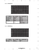
Page 88: ...ion and status is displayed upon receiving digital broadcast signal 6 2 1 13 DTV TUNING STATUS 3 6 2 1 14 DTV TV GUIDE BER TV Guide Bit Error Rate information 6 2 1 15 DEBUG INFO Debug information Note In the 29 32 rows the Boot version information on each device is displayed In the 19 24 rows the version of the execution program is displayed PANEL INFO It displays the generation of the panel inch...

Page 89: ...5 40 6 2 1 2 VERSION 2 6 2 1 3 VERSION 3 Meaning Item Name Display Example DTV Hardware Version HARDWARE XXXXXXXX DTV Hardware Serial SERIAL 01234567 DTV Runtime Version RUNTIME HHHHHHHH CFE Version CFE HHHHHHHH KERNEL Version KERNEL HHHHHHHH ROOTS Version ROOTS HHHHHHHH H W Y FLAGS FLAGS DVR Y FONTS Y DFAST Y PLOG Y N N I F O R E V R S I N 3 O M H G H G 0 1 2 3 4 5 6 7 A S P W S O R D 1 2 3 4 A M...

Page 90: ...nalog Tuner 1 MSPMAP MSP MAP FE2 Analog Tuner 2 AV SW AV Switch RGB SW RGB Switch VDEC VDEC SDRAM VDEC SDRAM ADC AD PLL HDMI HDMI US MSP FAN1 MSP RETRY DTV communication error DE BCM Abnormally in BCM7038 DE FE Tuner 1 or 2 DE CAS Card I F IC DE VBI VBI Slicer DE EPI EEPROM TV G TV Guide Error HOME G Failure at Home Gallery DTVMID Middleware DTVAPP Application MAIN Communication failure of Main mi...

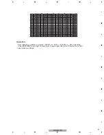
Page 91: ... N G N 8 A M T I O V D 1 3 1 0 6 0 N T V H A B 1 5 10 15 16 1 5 10 15 20 25 30 35 40 Operation Even if k key or l key is pressed CLEAR YES CLEAR NO is repeated If the ENTER SET key is kept on pressing for 5 second when the status of this menu is YES clear process will begin ...

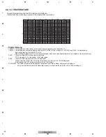
Page 92: ... F of the sensor becomes more than a specified temperature the shutdown start of processing FAN1 The value of the FAN rotating state is displayed STOP stopped LOW slow speed HIGH high speed FAN2 The value of the rotation state of FAN is displayed During a rotation of FAN 8bit D A value output from 2 pin DA0 of IF uCOM is displayed It is displayed with OFF during a stop only for the FHD model B SEN...

Page 93: ... _ _ _ _ _ _ _ _ 0 1 5 10 15 16 1 5 10 15 20 25 30 35 40 9 T I M E S B Meaning Item Name Display Example Corresponding RS 232C Command HOUR METER PANEL PANEL 00151H 21M QS3 POWER ON COUNTER P COUNT 00000095 TIMES QS3 HOUR METER MTB MTB 00151H 21M QS3 SYSTEM SERIAL SERIAL QS3 Display Meaning MTB HOUR METER N N I F O R T C M L E A R N O B H R U O M E R T E 8 A M T I O V D 1 3 1 0 6 0 N T V H A B 1 5...

Page 94: ...T C O L v D F A U L T R G B Q R E b 2 1 P I X D E P i t 1 5 10 15 16 1 5 10 15 20 25 30 35 40 N T V H A B Displays the input signal information of HDMI terminal Item Meaning PWR5V 5 V power detection 18 pin of HDMI terminal VSYNC VSYNC detection CKDT Clock detection SCDT SYNC detection DCRPT HDCP decryption status AUTHEN HDCP authentication status MODE HDMI mode status BIST NVAL N value CTSVAL CTS...

Page 95: ...ontal pixels decimal V RES Number of vertical lines decimal H DE Number of effectively horizontal pixels decimal V DE Number of effectively vertical lines decimal INTRL Interlace INT or progressive PRG V POL VSYNC polarity H POL HSYNC polarity AUDIO first line Sampling frequency ex DVD 48kHz CD 44 1kHz 1 AUDIO second line PCM PCM or No PCM no PCM AUDIO third line Quantization bit COL SP Color spac...

Page 96: ... system distinction result 096h ACC coefficient 098h 3D YC flag 1B5h MV detection 1 1B6h MV detection 2 1B7h MV detection 3 Sub Address Sub screen 400h 401h 494h 495h 496h 5B5h 5B6h 5B7h 6 2 1 9 VDEC SIGNAL INFO 1 N N I F O R D V E C I S NA L G N I O F D V M E C A M T I O C B A 3 1 2 0 6 0 2 0 0 0 2 0 0 0 2 0 0 0 2 0 0 0 2 0 0 0 5 8 B C D D V S E C 6 0 0 0 6 0 0 0 6 0 0 0 6 0 0 0 5 B 6 0 0 0 8 C D...

Page 97: ... P I D 3 0 2 2 0 1 2 0 1 2 0 8 1 I 1 6 9 0 D I G H A B 1 5 10 15 16 1 5 10 15 20 25 30 35 40 Displays digital broadcast signal information and status upon receiving digital signal 6 2 1 12 DTV TUNING STATUS 2 N N I F O R T D V T N U N G I A T S U S T B O O A T S T U C G A A M T I O C B A 3 1 3 0 6 0 E R F Q U E N C Y R O C R E C D E T E R R OR C N U O M I T E R R E E T C D E R R O R S 7 M 0 z H O ...

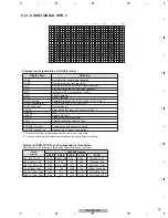
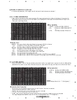
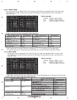
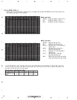
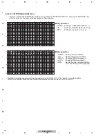
Page 98: ...yed with the hour meter values that indicate the hour values when power downs occurred 6 2 2 4 SHUT DOWN The shutdown history is displayed with the hour meter values that indicate the hour values when shutdowns occurred 6 2 2 5 PANEL 1 ADJ Settings of the driving pulse timing and driving voltage can be performed 6 2 2 6 PANEL 2 ADJ White balance and ABL power consumption for the panel can be set 6...

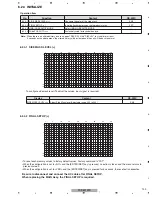
Page 99: ...anel product serial number and statuses of memories for adjustment values for the main unit and for backup are displayed No other layers are nested below this layer and there are no adjustment items MODULE The version of data written in the Module microcomputer IC3601 is indicated PRG The program version of the Module microcomputer is indicated DAT The data version of the Module microcomputer is i...

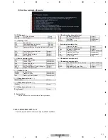
Page 100: ...ower down and corresponding OSD indications Cause of power down OSD Indication Cause of power down OSD Indication POWER SUPPLY Unit P PWR X DRIVE Assy XDRV SCAN Assy SCAN DC DC converter for X drive X DCDC 5 V power for SCAN Assy SCAN5V Y DRV X drive SUS circuit X SUS Y DRIVE Assy DC DC converter for Y drive Y DCDC Y drive SUS circuit Y SUS Digital DC DC converter D DCDC Unknown UNKNOWN ADDRESS As...

Page 101: ... the SUS FREQ setting has resulted in diminishing of AM radio interference in this layer after changing the setting turn the unit off then back on DOWN Shifting to PANEL 2 ADJ UP Shifting to POWER DOWN SET Shifting to the next nested layer g Key operation DOWN Shifting to the next item UP Shifting to the previous item RIGHT Adding by one to the adjustment setting value LEFT Subtracting by one from...

Page 102: ...screen to the next nested layer below for item selection Drive sequence and adjustment table Sequence Name Adjustment Value Table Video50 TBL2 6 2 2 6 PANEL 2 ADJ A P N E L L 1 B T 6 0 V S F A C T A J P N E L 2 A D A P N E L L 1 B T 6 0 V S F A C T R H G I H A J P N E L 2 A D 5 2 4 V D 1 1 5 0 6 0 N T V T A B V D 1 1 5 0 6 0 N T V T A B 1 5 10 15 16 1 5 10 15 20 25 30 32 1 5 10 15 16 1 5 10 15 20 ...

Page 103: ... Shifting to ETC UP Shifting to PANEL 2 ADJ SET Shifting to the next nested layer g Key operation DOWN Shifting to the next item UP Shifting to the previous item RIGHT Adding by one to the adjustment setting value LEFT Subtracting by one from the adjustment setting value SET Determining the adjustment setting value and shifting to the upper layer g Key operation A setting for panel degradation cor...

Page 104: ...P Shifting to PANEL FUNCTION SET Shifting to the next nested layer g Key operation DOWN Shifting to the next item UP Shifting to the previous item RIGHT Adding by one to the adjustment setting value LEFT Subtracting by one from the adjustment setting value SET Determining the adjustment setting value and shifting to the upper layer g Key operation The setting about the backup of panel adjusting va...

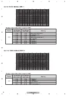
Page 105: ...tate Pressing the ENTER SET key shifts the screen to the next nested layer below for item selection DOWN Shifting to PATTERN MASK SETUP UP Shifting to ETC SET Shifting to the next nested layer The MASK indication sequence can be changed among 48V 50V 60V 72V 75V and 60P using the Right or Left key The selected sequence and the ABL WB table are retained until the mask is turned off DOWN Shifting to...

Page 106: ...ey The selected sequence and the ABL WB table are retained until the mask is turned off A P T T E R N M A S K S E T U P 6 2 2 10 PATTERN MASK SETUP DOWN Shifting to COMBI MASK SETUP UP Shifting to RASTER MASK SETUP SET Shifting to the next nested layer DOWN Shifting to the next MASK UP Shifting to the previous MASK RIGHT Changing MASK sequence LEFT Changing MASK sequence SET Determining the adjust...

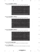
Page 107: ... key The selected sequence and the ABL WB table are retained until the mask is turned off O C M B I M A S K S E T U P 6 2 2 11 COMBI MASK SETUP DOWN Shifting to PANEL INFORMATION UP Shifting to PATTERN MASK SETUP SET Shifting to the next nested layer DOWN Shifting to the next MASK UP Shifting to the previous MASK RIGHT Changing MASK sequence LEFT Changing MASK sequence SET Determining the adjustme...

Page 108: ...ly used for production line 6 2 3 4 SYNC DET Exclusively used for technical analysis details omitted 6 2 3 5 CC Exclusively used for technical analysis details omitted No Function Content RS 232C 6 2 3 1 EDID WRITE MODE DISABLE ENABLE 6 2 3 2 ANTENNA MODE CABLE AIR 6 2 3 3 AFT OFF ON Controls AFT action 6 2 3 4 SYNC DET Exclusively used for technical analysis 6 2 3 5 CC Exclusively used for techni...

Page 109: ...el Adjustable range 000 to 255 SML N I I T I L A I Z E A T D A R E S T E I N F A L S E T U P V D 1 3 1 0 6 0 O N N T V H A B 1 5 10 15 16 1 5 10 15 20 25 30 35 40 6 2 4 2 FINAL SETUP 6 2 4 1 SIDE MASK LEVEL Be sure to disconnect and connect the AC cable after FINAL SETUP When replacing the MAIN Assy the FINAL SETUP is required Operation item No Function Content RS 232C 6 2 4 1 SIDE MASK LEVEL Conf...

Page 110: ...pment status If the ENTER key is kept on pressing for 5 second when the status of this menu is YES HMG HG SERVICE mode will be done 6 2 4 3 HMG HG SERVICE MODE 1 Home Gallery Screen 1 When the USB device is connected 2 When the USB device is not connected HG Home Gallery SERVICE MODE Regular model For ELITE model Be sure to do above procedure at input fuction except HMG For details refer to the se...

Page 111: ...duct revision number Hexadecimal 5 S String descriptor info 1 Manufacturer String 6 S String descriptor info 2 Product String String 7 S String descriptor info 3 SerialNumber 8 C Configuration descriptor info Ifs Number of Interfaces Decimal Cfg Configuration Number Decimal Atr Attributes Hexadecimal MxPwr MaxPower in mA Decimal 9 I Interface descriptor info If Interface Number Decimal Alt Alterna...

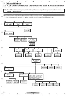
Page 112: ... the main parts and boards Power Button Case 508F 1 Side input cover 1 Function button panel 1 Rear case 508F 1 Terminal panel B 50U 3 Terminal panel A U 2 Side input panel 8U SIDE KEY Fan Holder Upper central part 4 Front case Assy 508FU FHD FAN CONNECT FHD POWER SW TANSHI 50FHD LED FHD RLS FHD IR SIDE IO 2 Side input shield 50F X DRIVE 50F Y DRIVE 2 Function button shield POD stay A POWER SUPPLY...

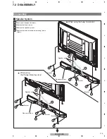
Page 113: ...using the hung on wall unit When using the Pioneer table top stand 2 Remove the three screws 3 Remove the speaker system 4 Remove the three brackets by removing the six screws 3 Speaker system Bracket Bracket Bracket 2 2 2 1 2 4 2 4 2 4 Speaker cable 3 Speaker system Bracket Bracket Bracket 2 2 2 1 2 4 2 4 2 4 Speaker cable ...

Page 114: ...tton case 508F 1 Remove the 20 screws AMZ30P060FTB 2 Remove the 10 screws TBZ40P080FTB 3 Remove the two screws ABA1332 4 Remove the one screw ABA1341 5 Remove the rear case 508F 1 Tighten the two screws 2 Tighten three screws 3 Tighten the two screws 4 Tighten the eight screws 5 Tighten other screws Rear case 508F Rear case 508F 5 1 1 1 1 1 1 1 1 1 2 2 2 2 3 2 2 2 2 3 2 2 1 1 1 1 1 1 1 4 1 1 1 1 1...

Page 115: ...ssy 1 1 2 POWER SUPPLY Unit PCB base NG OK FHD FAN CONNECT Assy For 50F X DRIVE Assy For 50F Y DRIVE Assy For SIDE IO Assy 3 Diagnose the 50F Y DRIVE Assy 3 Diagnose the 50F X DRIVE Assy Caution As the two capacitors on the 50F Y DRIVE Assy are located very close to sub frame L Assy 507 if the former Assy is tilted toward the latter Assy when disassembling they may come into contact with the latte...

Page 116: ...a fulcrum and the pliers as a lever pry the connector upward to remove it TANSHI Assy MAIN Assy 4 Terminal Panel B 50U 3 1 Remove the four screws 2 Remove the two screws 3 Remove the 10 screws 4 Remove the four screws 5 Remove the terminal panel B 50U 5 Terminal panel B 50U TANSHI Assy Terminal panel A U 3 1 3 3 2 2 3 3 3 3 3 1 2 3 3 4 4 4 4 The wiring shown in the photo is different from the actu...

Page 117: ...t to press the rivet Because when the rivet presses fit in once again Rivet 2 Pull the lower part of the Front case Assy 508FU toward you and out 3 Remove the Front case Assy 508FU by pulling it upward 2 3 Front case Assy 508FU Front side When assembling the front case tighten this rivet first 1 1 1 1 1 ...

Page 118: ...F DIGITAL Assy 5 2 Remove the two screws 3 Remove the four screws 1 Disconnect the cable Multi base section 2 3 1 3 3 3 2 4 Lift the Multi base section to the direction of the arrow Multi base section Multi base section PANEL SENSOR Assy 50F DIGITAL Assy 4 ...

Page 119: ...w 3 Remove the FHD RLS Assy 4 Remove the two screws 5 Remove the two screws 6 Remove the two screws 7 Remove the front chassis HB Assy 50 Front chassis HB Assy 50 1 Remove the two screws 2 Unhook the six hooks 3 3 3 Remove the panel holders V1 50 and V2 50 Panel holder V1 50 V2 50 1 2 2 1 1 1 6 1 5 5 1 1 1 2 3 7 3 Front chassis HT 508F Assy 50FHD LED Assy FHD IR Assy FHD RLS Assy 4 4 6 2 2 2 2 2 2...

Page 120: ...oosen the jumper wire 2 Remove the three screws 3 Remove the front chassis VL 508F Front chassis VL 508F SCAN IC 4 SCAN IC 4 SCAN IC 4 SCAN IC 4 Connecting Method Disconnecting Method Notes for Three pieces connector 40P Three pieces connector 40P is a precision part Pay attention to the handling In addition please do not touch the electrode plane OK OK OK NG NG NG NG ...

Page 121: ... not to bend the Grille Assy too far Otherwise it may be damaged OK Good example NG Bad example Reassembly Remove the old two sided tape attached to the rear side of the Grille Assy and the front side of the baffle and adhere new two sided tape Press the bosses into the baffle plate and press the entire grill into position Press the bosses from the woofer frame 2 Woofer Disassembly The woofer is s...

Page 122: ... Assy No adjustment required Refer to 8 3 HOW TO CLEAR HISTORY DATA and 8 6 PRECAUTION ON REPLACEMENT OF THE POWER SUPPLY UNIT MAIN Assy No adjustment required Service Panel Assy Refer to 8 3 HOW TO CLEAR HISTORY DATA and 8 4 ADJUSTMENTS WHEN THE SERVICE PANEL ASSY IS REPLACED Writing of backup data is required Refer to the 8 2 BACKUP OF THE EEPROM DIGITAL ASSY PANEL SENSOR Assy Writing of backup ...

Page 123: ...e whole Assy not only the defective part If any part listed below is identified as defective and needs replacement replace the whole Assy and make necessary adjustments after replacement Reason The whole Assy must be replaced because adjustments and data rewriting for the Assy at the level of production line are required PCB Assy No Assy Name Parts that Require Whole Assy Replacement Ref No Functi...

Page 124: ...play the PANEL INFORMATION page then check if NO DATA is set for DIG EEP and ADJUSTED is set for BACKUP Then proceed in the following steps 1 Copying using the Factory menu 1 Plug in the AC cord press the Power switch on the unit to set it to ON then enter Standby mode 2 Turn on the power using the remote control unit then enter Panel Factory mode Copy the backup data as shown in the figure below ...

Page 125: ...te data stored in the EEPROM on the DIGITAL Assy 3 Issue the BCP command to transfer the data stored in the EEPROM for backup 4 Turn the power off 3 Turn the power off Note If the secondhand DIGITAL Assy is mounted in the product then the unit is turned on then back off again the data in the EEPROM on the DIGITAL Assy are copied over the EEPROM in the PANEL SENSOR Assy Thus the backup data can nev...

Page 126: ...using Factory menu or RS 232C commands 1 Method using the Factory menu 1 Set various setting adjustment values 2 Proceed in the following steps 2 Method using the RS 232C commands Issue the FAJ command 3 Turn the power off Note When a DIGITAL Assy with an EEPROM in which adjustment data are stored is mounted this step is not required after manual adjustment DIGITAL EEPROM REPAIR is not indicated P...

Page 127: ...PRT BACKUP DATA NO OPRT DIGITAL EEPROM NO OPRT PD INFO NO OPRT PD INFO CLEAR MAX TEMP NO OPRT P COUNT INFO NO OPRT PM B1 B5 NO OPRT HR MTR INFO NO OPRT SD INFO NO OPRT Key Down 7th Key Down SET Right SET 5 sec SD INFO CLEAR Right SET 5 sec HR MTR INFO CLEAR Right SET 5 sec PM B1 B5 CLEAR Right SET 5 sec P COUNT INFO CLEAR Right SET 5 sec MAX TEMP CLEAR Right SET 5 sec Key Down Key Down Item Conten...

Page 128: ...he screen as shown in the figure below Make sure that 60VS is always indicated during adjustment Example of the On Screen display during Panel Factory mode Drive sequence indication Preparation In the PANEL 1ADJ layer the Panel White Balance value is reset to default Panel Gamma is set to Straight Noise is set to OFF LUT mode is set to ON and Reset active control is set to OFF In this case represe...

Page 129: ...voltage OK Checking VOL YNOFS3 4 1 min RST MASK 16 Green 1023 OK Checking VOL YNOFS3 4 1 min RST MASK 15 Red 1023 OK Checking VOL YNOFS3 4 1 max RST MASK 22 Cyan 3SF Main flowchart 2 VOL YNOFS check OK Checking VOL YNOFS3 4 1 min RST MASK 16 Green 1023 OK Checking VOL YNOFS3 4 1 min RST MASK 15 Red 1023 OK Checking VOL YNOFS3 4 1 max RST MASK 22 Cyan 3SF Main flowchart 1 VOL OFFSET check OK Checki...

Page 130: ... S00 To set the gamma R value to that for Factory mode PGG S00 To set the gamma G value to that for Factory mode PGB S00 To set the gamma B value to that for Factory mode DIZ S03 Dither ON L dither ON noise OFF 1800000001 LUT mode ON 1000003F00 Reset active control OFF Procedures for resetting corrections for change over time Perform aging for 5 minutes Enter the initial values for the panel for s...

Page 131: ...T MASK 03 Green MKS S53 Return VOL OFFSET to the tentative setting value VOF Determine the tentative setting value for VOL OFFSET as the final value Yes To the Recovery flowchart 1 3 No Yes To the Recovery flowchart 1 4 From the Recovery flowchart 1 2 and 1 4 Yes No To the Main flowchart 2 Is there erroneous discharge abnormal lit cell Check on the PANEL 1 ADJ menu Is there erroneous discharge abn...

Page 132: ...inal value From the Recovery flowchart 2 1 and 2 3 Note Make sure that the following values become the final setting values VOL SUS 1 VOL XPOSF2 1 VOL OFFSET VOL YNOFS1 VOL RST P 1 VOL YNOFS3 VOL XPOFS1 1 VOL YNOFS4 1 The tentative setting value becomes the final value To the Recovery flowchart 2 1 Yes Is there erroneous discharge abnormal dead cell Check on the PANEL 1 ADJ menu Display RST MASK 2...

Page 133: ...urrent setting value plus 112 VOF Gradually increase the VOL OFFSET value until disappear the discharge lit cell The VOL OFFSET value must be 133 or less Current VOL OFFSET 133 To the Recovery flowchart 1 2 Display RST MASK 02 Red MKS S52 Replacement of abnormal circuits or re replacement of the panel required Replacement of abnormal circuits or re replacement of the panel required No Yes Graduall...

Page 134: ...termine the current VOL OFFSET setting value as the final value Replacement of abnormal circuits or re replacement of the panel required Replacement of abnormal circuits or re replacement of the panel required No Yes Gradually decrease the VOL OFFSET value until disappear the discharge dead cell The VOL OFFSET value must be 117 or greater Current VOL OFFSET 117 No Yes Is there erroneous discharge ...

Page 135: ...crease the VOL OFFSET value until disappear the discharge dead cell The VOL OFFSET value must be 117 or greater Current VOL OFFSET 117 To the Main flowchart 2 Set VOL OFFSET to the current setting value plus 64 VOF Determine the current VOL OFFSET setting value as the final value Replacement of abnormal circuits or re replacement of the panel required No Yes Is there erroneous discharge abnormal d...

Page 136: ...e panel required No Yes Yes To the Recovery flowchart 2 2 From the Recovery flowchart 2 2 Yes Current VOL YNOFS3 setting value 137 No Is there erroneous discharge abnormal dead cell No Is there erroneous discharge abnormal dead cell Set VOL YNOFS4 to the current setting value 4 VY4 Display RST MASK 22 Cyan 3SF MKS S72 Set VOL YNOFS3 to the current setting value 47 VY3 Set VOL YNOFS4 to the current...

Page 137: ... 4 VY3 Set VOL YNOFS1 to the current setting value VY1 Set VOL YNOFS4 to the current setting value plus 4 VY4 To the Recovery flowchart 2 1 B Adjustment completed Set VOL YNOFS1 to the final setting value of VOL YNOFS3 minus 31 VY1 Determine the current VOL YNOFS1 setting value as the final value VOL YNOFS3 final setting value Note Make a note of this VOL YNOFS3 value From the Main flowchart 2 Rec...

Page 138: ...VOL YNOFS4 to the current setting value plus 23 VY4 Set VOL YNOFS3 to the current setting value minus 47 VY3 Set VOL YNOFS4 to the current setting value minus 47 VY4 RST MASK 22 Cyan 3SF Display RST MASK 16 Green 1023 MKS S66 No Yes Is there erroneous discharge abnormal dead cell Check on the PANEL 1 ADJ menu Replacement of abnormal circuits or re replacement of the panel required No Yes Is there ...

Page 139: ...54 40 139 172 049 187 057 177 057 177 057 41 144 173 051 188 059 178 059 178 059 42 149 174 053 189 061 179 061 179 061 43 155 175 055 190 063 180 063 180 063 44 160 176 057 191 065 181 065 181 065 45 165 177 058 192 067 182 067 182 067 46 171 178 060 193 069 183 069 183 069 47 176 179 062 194 072 184 072 184 072 48 181 180 064 195 074 185 074 185 074 49 187 181 066 196 076 186 076 186 076 50 192 ...

Page 140: ...89 236 166 250 191 240 191 240 191 237 168 251 193 241 193 241 193 238 170 252 195 242 195 242 195 239 172 253 197 243 198 243 198 240 174 254 200 244 200 244 200 241 176 255 202 245 202 245 202 242 177 256 204 246 204 246 204 243 179 257 206 247 206 247 206 244 181 258 208 248 208 248 208 245 183 259 210 249 210 249 210 246 185 260 212 250 212 250 212 247 187 261 214 251 214 251 214 248 188 262 2...

Page 141: ...S U signal input to the DRIVE Assy SUS B signal input to the DRIVE Assy SUS U Gate signal SUS B Gate signal X DRIVE Gate terminal of Q1220 Y DRIVE Gate terminal of Q2217 X DRIVE Gate terminal of Q1109 Y DRIVE Gate terminal of Q2107 50 of the crest value time lag of SUS U and SUS B Δ Tsus iub time lag of SUS U Gate and SUS B Gate Δ Tsus gub Assy VR Value of α X DRIVE Assy VR1002 70 nsec Y DRIVE Ass...

Page 142: ...e pulse width 5 nsec as the SUS D signal Note Be sure to set the Drive to OFF for adjustment For details on measuring points of waveform see the figure below 50 of the crest value 50 of the crest value 50 of the crest value 50 of the crest value SUS D pulse width Tsus Dg Adjust so that Tsus Dg Tsus D 5 nsec using the variable control shown in the table below SUS D signal input to the DRIVE Assy SU...

Page 143: ... TP1258 Q1204 Y DRIVE Assy Y DRIVE Assy 1 Measure the SUS D pulse width Tsus D 2 Adjust the pulse width Tsus Dg of the SUS D input signal so that it becomes Tsus D 5 nsec from DIGITAL Assy YSUS D IC2005_A7 Q2105 VR2001 IC2104 Q2111 IGBT TP2114 Q2113 IGBT TP2116 YSUS U from DIGITAL Assy IC2001_A4 Pin 5 IC2101 IC2103 Q2106 IGBT Q2107 IGBT Q2104 Photo Coupler TP2106 TP2107 Q2108 IGBT TP2108 Q2109 IGB...

Page 144: ...6 from the old one and attach it to the new one NEVER turn on the unit before replacement as doing so may damage the PC boards or the product POWER SUPPLY unit POWER SUPPLY unit old POWER SUPPLY unit new P11 P11 1 1 2 Housing wire J126 Housing wire J126 Disconnect the housing wire J126 from the P11 terminal on the old POWER SUPPLY Unit 2 Connect the housing wire J126 to the P11 terminal on the new...

Page 145: ...n for control 232C cable straight The setting of the Com port cannot be communicated if it doesn t do correctly Please follow a set explanation of PC in the Com port Individual ports are provided for RS 232C and SR connectors with this model Therefore unlike the case of previous models which required switching of exclusive operation between these connectors on the Integrator menu switching is no l...

Page 146: ...uner preset channel 1 step reverse CHR Clearing data of the hour meter of MTB side CNT User contrast CMT Clearing data of the maximum temperature CPC Clearing power on count data CPD Clearing power down histrory CPM Clearing data of the pulse meter CSD Clearing shutdown history CTM Releasing the TRAP SW DW To subtract to the adjustment value 000 to 999 designated by a function command DRV DIZ S00 ...

Page 147: ...g S06 S00 S01 S02 S03 S04 S05 S06 S07 Input switch INPUT 8 PC S08 S01 S02 S03 MIR Mirror mode OFF default Mirror mode Right and left inversion Mirror mode Top and bottom inversion Mirror mode Top and bottom and right and left inversion S00 S01 S02 S03 S04 S05 Erasing afterimage 1 S07 Erasing afterimage 2 S08 White change in luminance level S09 PEAK detection raster MKS S10 Address lack check Mod S...

Page 148: ...ar S29 RGB checker 1 S30 S31 S32 S33 S34 S35 S36 S37 S38 S39 RGB checker 2 Window GREEN GREEN 1023 Even line horizontal stripes Window BLUE BLUE 1023 Window RED RED 1023 Afterimage check 2 Afterimage check 4 Mod S40 Red single color slanting ramp Mod S41 GREEN single color slanting ramp Mod S42 BLUE single color slanting ramp Mod S43 For panel light check 1 Mod S44 For panel light check 2 Mod S45 ...

Page 149: ... S10 Panel drive mode OPTIMUM Main Main N OSD S00 Turning OSD setting to off S01 Turning OSD setting to on O Mod Mod Mod Mod Mod Mod Mod Mod Mod Mod Mod Mod Mod Mod Mod Mod Mod Mod Mod Raster Cyan S57 S56 Raster Magenta S58 Raster Yellow S59 Raster Pink S60 Raster Cyan 291 S61 Raster Yellow egg color S62 Raster Light blue MST Display one screen S01 S00 PsideP Main size normal S02 PinP Right down S...

Page 150: ...mand Name Function Effective only in Factory mode Active U com Last Memory Remarks MDU MTB P S01 Blue independent gamma setting Fixed on 1 6 S02 Blue independent gamma setting Fixed on 1 7 S03 Blue independent gamma setting Fixed on 1 8 S04 Blue independent gamma setting Fixed on 1 9 S05 Blue independent gamma setting Fixed on 2 0 S06 Blue independent gamma setting Fixed on 2 1 S07 Blue independen...

Page 151: ...cquiring unit data such as the software version common to all models regardless of destination QS3 Acquiring data on the status of the unit such as temperature QS2 QSE Acquiring unit data such as the software version common to all models regardless of destination QSD Acquiring data on shutdown Q S01 Red independent gamma setting Fixed on 1 6 S02 Red independent gamma setting Fixed on 1 7 S03 Red i...

Page 152: ...ng for panel degradation correction LV6 BLUE setting for panel degradation correction LV7 Mod Mod Mod Mod Mod Mod Mod S00 RGL GREEN setting for panel degradation correction Lv0 no correction Mod S01 S02 S03 S04 S05 S06 S07 GREEN setting for panel degradation correction LV1 GREEN setting for panel degradation correction LV2 GREEN setting for panel degradation correction LV3 GREEN setting for panel ...

Page 153: ...NG correction mode 4 STREAKING correction mode 5 STREAKING correction mode 6 STREAKING correction mode 7 S01 S03 Setting of the effective area during streaking correction 4 3 detection Setting of the effective area during streaking correction D BY D detection VGA S02 Setting of the effective area during streaking correction 14 9 detection S04 Setting of the effective area during streaking correcti...

Page 154: ... ZME ZPR Initializing the video EEPROM data Initializing the setting data to which no adjustment command is provided PANEL EEPROM REFLESH W X Y Z Mod X3B 2SF third XSUS resonance up width Mod X1B 3SF and later first XSUS resonance up width VFQ S01 Setting the frequency in Mask mode to VD 48 Hz S02 Setting the frequency in Mask mode to VD 50 Hz S03 S05 S06 S13 S23 Setting the frequency in Mask mode...

Page 155: ...of IF microcomputer 8 byte 22 Boot version of IF microcomputer 4 byte Program version of Main microcomputer 8 byte 23 Boot version of Main microcomputer 4 byte 24 Program version of ASIC 8 byte 25 Boot version of ASIC 4 byte CS Check Sum 2 byte 5 Panel Product Form S System model B All in one design TV M Monitor D Standard module E Simple module 15 MTB Generation 6 G6 7 G7 8 G8 9 G9 0 G10 16 MTB D...

Page 156: ...t not completed 3 Adjustment data backup flag 0 With backup data 1 No backup data 4 5 PD data 0 No PD data 1 Not used 2 POWER 3 SCAN 4 SCN 5V 5 Y DRV 6 Y DCDC 7 Y SUS 8 ADRS 9 X DRV A X DCDC 9 1 SD Sub SQ_LSI 0 No SD Sub data 1 Communication error 2 Drive stop 3 BUSY 4 Version mismatching H S B X SUS C DIG DCDC D Not used E Not used F UNKNOWN 8 SD main data 0 No SD 1 SQ_LSI communication error 2 M...

Page 157: ...TEMP1 acquisition Temperature value 5 byte 25 0 1 6 TEMP0 acquisition Temperature value 5 byte 25 0 1 7 MaxTEMP acquisition Temperature value 5 byte 75 0 1 8 9 Reserved 4 byte CS 2 byte FB Command Format Effective Operation Modes Function Remarks QS3 All operations To acquire data on operations of the panel Return data 3 ECO 58 DATA 2 CS 63 Byte The command QS3 is for acquiring data on operational...

Page 158: ...ment value 3 byte 128 18 YTK adjustment value 3 byte 128 19 YTZ adjustment value 3 byte 128 20 Y2K adjustment value 3 byte 128 24 R REVISE setting value 1 byte 0 25 G REVISE setting value 1 byte 0 26 B REVISE setting value 1 byte 0 21 Y2Z adjustment value 3 byte 128 22 YNK adjustment value 3 byte 128 23 YNZ adjustment value 3 byte 128 27 ADDRESS 1 2 setting value 2 byte 01 30 ADDRESS 7 8 setting v...

Page 159: ...ness by protective operations 0 Upper limit state for brightness 1 Brightness being reduced 2 Lower limit state for brightness 3 Brightness being increased 17 WB interlocked with APL 0 OFF 1 ON 2 WB interlocked ON γ OFF 3 WB interlocked OFF γ ON 1 Drive sequence 50V Video 50 Hz 48V Video 48 Hz 60V Video 60 Hz 72V Video 72 Hz 75V Video 75 Hz 70P PC 70 Hz 60P PC 60 Hz 2 Standard nonstandard S Standa...

Page 160: ...data 1 byte 0 15 Data from the hour meter for the fifth latest PD 8 byte 00000715 16 Sixth latest 1st PD data 1 byte A 17 Sixth latest 2nd PD data 1 byte 2 18 Data from the hour meter for the sixth latest PD 8 byte 00000552 19 Seventh latest 1st PD data 1 byte A 20 Seventh latest 2nd PD data 1 byte 0 21 Data from the hour meter for the seventh latest PD 8 byte 00000213 22 Eighth latest 1st PD data...

Page 161: ... latest SD subcategory data 1 byte 2 18 Data from the hour meter for the sixth latest SD 8 byte 00045662 19 Seventh latest SD data 1 byte 0 20 Seventh latest SD subcategory data 1 byte 0 21 Data from the hour meter for the seventh latest SD 8 byte 00000000 22 Eighth latest SD data 1 byte 0 23 Eighth latest SD subcategory data 1 byte 0 24 25 Data from the hour meter for the eighth latest SD 8 byte ...

Page 162: ...5 1 byte 12 FLAGS Information 6 1 byte 13 HMG HG Model Version 10 byte 14 User Password 4 byte 15 Check Sum 2 byte Command Format Effective Operation Modes Function Remarks QSE Every time Output of status Induce it peculiar individual information is acquired Data Arrangement Part Order Data Length Output Example Received Command name 3 byte QMT 267 1 009 5 1 0 MTB A D value of MTB side Temperature...

Page 163: ... 1 byte 11 MTB hour meter for the 3rd latest NG 7 byte 12 Reserved 3 byte 29 8th latest NG No 1 byte 30 Subcategory No for the 8th latest NG 1 byte 31 MTB hour meter for the 8th latest NG 7 byte 32 Reserved 3 byte 33 Check Sum 2 byte Frequency Part Part Remarks Operation MTB part Immediately Shutdown Immediately Shutdown 5 Shutdown signal from audio amp short circuit of speaker terminal Shutdown a...

Page 164: ...ication error of IF microcomputer Shutdown 2 Communication error of sequence processor Shutdown No 10 Subcategory Information on Abnormally in FAN Value Shutdown Factor Remarks Operation 1 FAN 1 Shutdown 2 FAN 2 FHD only Shutdown No 12 Subcategory Information on Failure in Digital Tuner Value Shutdown Factor Remarks Operation 1 DTV starting failure Turn off the screen then reset the device 2 DTV c...

Page 165: ...tive Operation Modes Function Remarks QSI All operations To acquire all data on input video signals Return data 3 ECO 66 DATA 2 CS 71 Byte The command QSI is for acquiring all data on input video signals 18 to 21 Each protection function 0 Setting OFF 2 Setting ON during operation 1 Setting ON during wait 22 Transition of protection operations 0 Upper limit state for brightness 1 Brightness being ...

Page 166: ...CE FACTORY MODE FAN During FAY Adjustment command is invalid Command Format Operation Remarks Effective Operation Modes Control FAJ During FAY To make the flag setting that indicating that adjustment of the panel unit has been completed This takes at least 350 mS UAJ To make the flag setting that indicating that adjustment of the main unit has not been completed CBU To make the flag setting that i...

Page 167: ...PDP 5010FD 167 5 6 7 8 5 6 7 8 C D F A B E ...

Page 168: ...e component parts indicates the importance of the safety factor of the part Therefore when replacing be sure to use parts of identical designation Screws adjacent to mark on product are used for disassembly For the applying amount of lubricants or glue follow the instructions in this manual In the case of no amount instructions apply as you think it appropriate NOTES Speed clamp 3 Bead band 3 Scre...

Page 169: ...A2634 19 Pad 508F REG T R AHA2635 20 Pad 508F REG ACC AHA2675 21 Under Carton See Contrast table 2 22 Upper Carton 5010FD See Contrast table 2 23 Packing Sheet L See Contrast table 2 24 Band Assy AXY1192 25 Speaket System SMW1985 26 HDMI Caution See Contrast table 2 27 28 Parental Caution See Contrast table 2 Mark No Description Part No Mark No Symbol and Description PDP 5010FD KUCXC PDP 5010FD KU...

Page 170: ...PDP 5010FD 170 1 2 3 4 1 2 3 4 C D F A B E 10 2 REAR SECTION B B A A TANSHI CN8801 CN8802 MAIN CN4110 USB C C MAIN CN4109 Refer to 10 3 FRONT SECTION ...

Page 171: ...Label C U AAX3501 22 Label B50 U AAX3540 23 Terminal Panel B 50U ANC2452 24 Power Button Case 508F AAK2908 25 Function Button Panel AMB2906 26 Side Input Cover AMB2911 27 Function Button AAC1562 28 Power Button 508F AAD4152 29 Function Button Sheet 8U AAK2919 30 Input Cover Label 8U AAX3509 31 Rear Case 508F ANE1662 32 Cushion AEB1489 33 34 Screw 3 x 40P ABA1332 35 Screw ABA1341 36 Screw AMZ30P060...

Page 172: ...PDP 5010FD 172 1 2 3 4 1 2 3 4 C D F A B E 10 3 FRONT SECTION MAIN CN4107 MAIN CN4109 Rear view Refer to 10 4 CHASSIS SECTION 1 2 ...

Page 173: ...WW1289 2 50FHD LED Assy AWW1291 3 FHD RLS Assy AWW1292 4 6P 6P 3P Housing Wire J117 ADX3562 5 Blind Cushion 508F AEB1479 6 Nylon Rivet AEC1671 7 Rivet AEC1877 8 1 Front Case Assy 508FU AMB3001 NSP 9 2 Panel Cushion H 50 AED1257 NSP 10 2 Panel Cushion V 50 AED1258 11 12 FC Gate Sheet AMR3746 13 Screw ABZ30P080FTC ...

Page 174: ...B E 10 4 CHASSIS SECTION 1 2 FHD FAN CONNECT CN9553 MAIN CN4103 POWER SUPPLY P10 FHD FAN CONNECT CN9555 FHD FAN CONNECT CN9554 Cleaning liquid GEM1004 Cleaning paper GED 008 Refer to 10 7 MULTI BASE SECTION Refer to 10 5 CHASSIS SECTION 2 2 ...

Page 175: ...092 11 Front Chassis HB Assy 50 ANA2094 12 Panel Holder V1 50 ANG2770 13 Panel Holder V2 50 ANG2771 14 Fan Holder ANG2833 15 Multi Base Holder ANG2937 16 Sub Frame Plate ANG3046 17 Floating Rubber 80 AEB1427 18 Ferrite Core Holder AEC1818 19 Reuse Wire Saddle AEC1945 20 Ferrite Clamp AEC1986 21 Reuse Wire Saddle AEC2118 22 Fan Holder AMR3704 23 Gasket ADH FCH ANK1850 24 25 26 Screw See Contrast ta...

Page 176: ...HASSIS SECTION 2 2 I Q R S O S T V V D C B A X J H I G F W E Y Y J L K L K M N A B O P D C N M U U X Q R E P F T G H W MAIN CN4101 MAIN CN4105 MAIN CN4106 TANSHI CN8806 FHD POWER SW CN9571 AC Inlet MAIN CN4113 Fan 3 Refer to 10 6 PANEL CHASSIS SECTION ...

Page 177: ...8 Flexible Cable J210 ADD1507 19 Flexible Cable J211 ADD1508 20 5P Housing Wire J105 ADX3359 21 Housing Wire J126 ADX3545 22 9P 7P Housing Wire J101 ADX3550 23 8P 8P Housing Wire J102 ADX3551 24 14P Housing Wire J104 ADX3553 25 6P 6P Housing Wire J108 ADX3556 26 6P 6P Housing Wire J109 ADX3557 27 6P 6P Housing Wire J111 ADX3558 28 6P 6P Housing Wire J112 ADX3559 29 3P 3P 3P Housing Wire J123 ADX35...

Page 178: ...PDP 5010FD 178 1 2 3 4 1 2 3 4 C D F A B E 10 6 PANEL CHASSIS SECTION ...

Page 179: ...CAN B Assy AWW1313 NSP 6 50F SCAN C Assy AWW1314 NSP 7 50F SCAN D Assy AWW1315 NSP 8 Plasma Panel 50F Assy AWU1235 9 PCB Spacer Reuse AEC2087 10 PCB Spacer Reuse AEC2122 11 Heat Radiation Sheet AEH1134 12 Conductive Plate Holder AMR3446 13 Address Plate 50F A ANG3048 14 Address Plate 50F B ANG3071 15 Conductive Plate X F ANG2906 16 Screw ABA1351 17 Screw ABA1364 18 Three Pieces Connector 40P AKM13...

Page 180: ...D F A B E 10 7 MULTI BASE SECTION A B B D USB side Fan FHD FAN CONNECT CN9551 P9 P8 POWER 50F DIGITAL CN3201 SIDE KEY CN9501 FHD IR CN9731 FHD RLS CN9781 50FHD LED CN9671 POWER P3 SIDE IO CN9352 SIDE IO CN9351 E D E F F C C POWER P5 A ...

Page 181: ...5 11 11 6 4P Housing Wire J114 ADX3560 12 13 11P Housing Wire J118 ADX3563 14 8P 4P Housing Wire J119 ADX3531 15 7P Housing Wire J125 ADX3566 16 3P Housing Wire J127 ADX3546 17 18 Locking Card Spacer AEC1429 19 Wire Saddle AEC1745 20 Reuse Wire Saddle AEC1945 21 Silicone Sheet Audio AEH1143 22 POD Cover AMR3542 23 Multi Base Assy U ANA2102 24 Terminal Panel A U ANC2440 25 POD Stay A ANG2933 26 27 ...

Page 182: ...PDP 5010FD 182 1 2 3 4 1 2 3 4 C D F A B E 10 8 PDP SERVICE ASSY 508F AWU1272 Exterior Section ...

Page 183: ...s Plate 50F B ANG3071 12 Rivet AEC1877 13 Ferrite Clamp AEC1986 14 Side Type Mini Clamp AEC2003 15 PCB Spacer Reuse AEC2122 16 Gasket ADH FCH ANK1850 17 Gasket AD ANK1948 NSP 18 Front Case 508F AMB3000 19 Rear Case 508F ANE1662 NSP 20 Drive Voltage Label ARW1097 21 Screw 3 x 40P ABA1332 22 Screw ABA1351 23 Screw ABA1364 24 Screw ABZ30P080FTC 25 Screw AMZ30P060FTB 26 Screw APZ30P080FTB 27 Screw TBZ...

Page 184: ...10 9 TABLE TOP STAND TABLE TOP STAND PARTS LIST Front Rear Bottom view Mark No Description Part No 1 Base Cover Assy AXY1176 2 Stand Pipe L Assy AXY1182 3 Stand Pipe R Assy AXY1183 4 Screw ABA1357 5 Screw M8 x 23 ABA1371 6 Screw M8 x 40 ABA1373 ...

Page 185: ...1127 8 2 Gasket SED1136 9 2 Gasket SED1138 10 2 Gasket SED1166 NSP 11 2 Bracket LR SNA1481 12 1 Bracket Assy C SXG1128 13 2 Gasket SED1140 14 2 Gasket SED1141 15 2 Gasket SED1167 NSP 16 2 Bracket C SNA1482 17 18 Protector Side SHA2577 19 Protector C T SHA2578 20 Protector C M SHA2579 21 Protector C B SHA2580 22 Protection Sheet S3 SHC1846 23 Protection Sheet S1 SHC1847 24 Packing Case SHG2780 25 P...

Page 186: ...86 1 2 3 4 1 2 3 4 C D F A B E 10 11 CS ASSY Baffle back Grille back Baffle Front Grille Front Cabinet inside Top Top Top Section A Rear Top Tweeter Input Terminal Input Terminal TW WF TW WF TW WF TW WF WF TW TW FW ...

Page 187: ...092 NSP 20 Gasket SEC2093 NSP 21 Gasket SEC2113 NSP 22 Gasket SEC2114 NSP 23 Gasket SEC2150 NSP 24 Gasket SEC2142 NSP 25 Felt SED1127 NSP 26 Felt SED1130 27 Tape SEH1089 28 Tape SEH1099 29 Tape SEH1117 30 Input Terminal SKX1098 NSP 31 MDF Bar SLX1165 NSP 32 Paper Tube 26 SMR1403 NSP 33 Acoustic Absorbent SMT1331 NSP 34 Acoustic Absorbent SMT1333 NSP 35 Acoustic Absorbent SMT1335 NSP 36 Acoustic Ab...

Reviews: