PDP-501MX, PDP-V501X
83
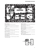
+5V Generation Point
D2604 anode
D2703 anode
D3104 anode
D3209 anode
D3320 anode (YA)
D3310 anode (YB)
D3322 anode (YA)
D3324 anode (YB)
ASSY Name
X DRIVE(A)ASSY
X DRIVE(B)ASSY
Y DRIVE(A)ASSY
Y DRIVE(B)ASSY
POWER SUPPLY
MODULE
Operating PD
VCP+12V over-current
(+) reset circuit over-
current
VCP+12V over-current
(–) reset circuit over-
current
VH150V over-current
VH150V over-current
PD only at small signal
block
(Large Power line off)
Note)
PD at the large power
block
V
CSP
+40V
V
SUS
+175V
V
OFS
+150V
V
RN
–190V
Faulty Point
•
Pulse module IC2610, IC2611 peripheral circuit
•
(+) reset circuit Q2702 peripheral circuit
•
Q2702G-S signal
•
X
PR-U
signal terminal K2611 (5V amplitude)
•
Pulse module IC3101, IC3106 peripheral circuit
•
Y
SUS_MSK
FET-Q3206-Q3209 peripheral circuit
•
C
SP_MSK
FET-Q3005-Q3006 peripheral circuit
•
Scan assembly internal bypass FET
Q7701, Q7702 peripheral circuit
•
Y
NR_D
output FET Q3204 peripheral circuit
•
Y
NR_U
output FET Q3201 peripheral circuit
•
Q3204 G-S control signal
•
Q3201 G-S control signal
•
Y
NR_D
signal terminal K3117
•
Y
NR_U
signal terminal K3118
•
D-D converter circuit mis-operations
•
When short-circuited between VH150V and
GND
•
Scan IC fault
•
D-D converter fault
•
When not short-circuited between VH150V and
GND
•
VH over-current mode (BYPASS FET is
always ON)
•
BYPASS output FET short-circuited
•
Digital section BYPASS control signal fault
•
Control signal stuck
•
VH over-current mode (Scan IC mis-
operations)
•
Scan IC fault
•
Scan IC control signal fault
•
V
SUS
175V line fault
•
When small signal block power overload
•
Fault of small signal block power supply of
assemblies
•
Fault of only the POWER SUPPLY MOD.
•
When not small signal block power overload
•
Fault of the POWER SUPPLY MOD. when PD
occurs in the POWER SUPPLY MOD. alone
•
Fault of assembly when PD does not occur in
the POWER SUPPLY MODULE alone
•
When large power block overload
•
Fault of power supply of each drive assemblies
•
Fault of the POWER SUPPLY MOD.
•
When not large power block overload
•
Fault of the POWER SUPPLY MOD. when PD
occurs in the POWER SUPPLU MOD. alone
•
Drive circuit mis-operations when PD occurs
due to drive assembly operations
•
Drive control signal fault
•
Pulse module IC input signal fault
Between SUS-B
4
and
6
of IC2610 (XA)
Between SUS-U
5
and
6
of IC2611 (XB)
Between SUS-D
!
and
@
of IC3101-1 (YA)
Between SUS-G
*
and
(
of IC3106 (YA)
•
Fault between FET and G of each output
TP NO.
When K2609 is H
When K3109 is H
When the following
are L
P12 Pin
5
(PD.XA)
Pin
7
(PD.XB)
P6 Pin
8
(PD.YA)
Pin
0
(PD YB)
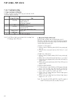
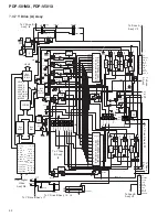
3. Diagnosis of Malfunctions when Power Down (PD) Occurs
Note) If PD occurs w5V supplied to the PD terminal of the drive assembly, overload of the power supply or malfunction of the POWER
SUPPLY MOD. may be suspected. Turn OFF the large power ON/OFF switch SW1 of POWER SUPPLY MOD., and short-circuit Pins
1
to
3
of CN3305 of each assembly of Y DRIVE (A)/(B) so that only the small signal block can be checked.
Summary of Contents for PDP-501MX
Page 16: ...PDP 501MX PDP V501X 16 A B C D 1 2 3 4 1 2 3 4 3 3 POWER SUPPLY MODULE 1 2 J 1 2 ...
Page 17: ...PDP 501MX PDP V501X 17 A B C D 5 6 7 8 5 6 7 8 J 1 2 ...
Page 18: ...PDP 501MX PDP V501X 18 A B C D 1 2 3 4 1 2 3 4 3 4 POWER SUPPLY MODULE 2 2 J 2 2 ...
Page 19: ...PDP 501MX PDP V501X 19 A B C D 5 6 7 8 5 6 7 8 J 2 2 ...


