background image

PDP-505MX

80

1

2

3

4

1

2

3

4

C

D

F

A

B

E

1

2 3

5

4

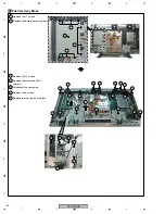
Front Panel Assy

2

• The following are order to remove a Bezel part.

1. Remove the Back Cover.
2. Remove the Frame Assy.
3. Remove the PDP module Assy.
4. Remove the BRACKET FILTER T .
5. Remove the Front panel including a glass filter.
6. Remove the bezel part is completed.

Remove the rear panel cover (Back Cover).

 (Screw 4*12 *31 pcs)

(Screw 3*6*9 pcs)

BACK COVER(50XM3)

(HANDLE *4 pcs)

 Remove the Frame Assy and the PDP module

Remove above pointed screw, 16 pcs, and 2 connectors.
After that, separate Frame Assy and Front Assy.

(Remove the connector)

(Remove the connector)

(Screw 4*12 *16pcs)

 Remove below pointed screws. After that,

 remove "BRACKET FILTER T".

Remove 2 screws for holding FRONT PANEL. 

After that, remove the Bezel part.

(4*12 *6pcs)

(Screw 4*8 *5pcs)

BRACKET FILTER T

The Bezel part

(Screw 4*12 *2pcs)

 The screen of a set puts downward. (Remove the Stand.)

Summary of Contents for PDP-505MX

Page 1: ... PIONEER ELECTRONICS ASIACENTRE PTE LTD 253 Alexandra Road 04 01 Singapore 159936 PIONEER CORPORATION 2006 PDP 505MX ARP3411 PLASMA DISPLAY PDP 505MX PDP 50FXE10 THIS MANUAL IS APPLICABLE TO THE FOLLOWING MODEL S AND TYPE S Model Type Power Requirement Remarks PDP 505MX KUCXZC AC 120 V PDP 50FXE10 TLXZC5 AC 100 to 240 V For details refer to Important Check Points for good servicing T IZY SEPT 2006...

Page 2: ...e put back in place such as barriers nonmetallic knobs adjustment and compartment covershields isolation resistor capacitor etc 3 When service is required observe the original lead dress Extra precaution should be taken to assure correct lead dress in the high voltage circuitry area 4 Always use the manufacture s replacement components Especially critical components as indicated on the circuit dia...

Page 3: ...not exceed 1mA ANY MEASUREMENTS NOT WITHIN THE LIMITS OUTLINED ABOVE ARE INDICATIVE OF A POTENTIAL SHOCK HAZARD AND MUST BE CORRECTED BEFORE RETURNING THE SET TO THE CUSTOMER PRODUCT SAFETY NOTICE Many electrical and mechanical parts in PIONEER set have special safety related characteristics These are often not evident from visual inspection nor the protection afforded by them necessarily can be o...

Page 4: ...the product Please check that neither solder debris nor screws remain inside the product 8 There should be no semi broken wires scratches melting etc on the coating of the power cord Damaged power cords may lead to fire accidents so please be sure that there are no damages If you find a damaged power cord please exchange it with a suitable one 9 There should be no spark traces or similar marks on ...

Page 5: ...K DIAGRAM 16 3 2 SYSTEM BLOCK DIAGRAM 18 3 3 PS251 PWR BLOCK DIAGRAM 19 3 4 BLOCK DIAGRAM OPERATION EXPLANATION 20 3 5 SCHEMATIC DIAGRAM 22 3 6 WAVEFORMS 52 4 PCB DIAGRAM 54 5 PCB PARTS LIST 58 6 ADJUSTMENT 61 7 GENERAL INFORMATION 76 7 1 SHUTDOWN 76 7 2 SPECIFICATIONS ON TEMPERATURE SENSOR DETECTION AND DRIVING OF THE FAN 77 7 3 TROUBLE SHOOTING 78 8 DISASSEMBLY 79 9 DIAGNOSIS OF THE PDP MODULE 8...

Page 6: ...1 S video S video DIN 4 pin x 1 Audio Stereo RCA x 2 INPUT5 Component RCA pin Y Pb Cb Pr Cr x 1 Audio Stereo RCA x 2 RS 232C D sub 9 pin x 1 Sound Output 8 W 8 W at 6 ohm Power Supply AC 120 V 60Hz Current Rating 3 5 A Standby Power Consumption 1 7 W Dimensions 1222 W x 740 H x 96 D mm Including handles Weight 44 kg Environmental Considerations Operating Temperature 0 C to 40 C 32 F to 104 F EMI C...

Page 7: ...PDP 505MX 7 5 6 7 8 5 6 7 8 C D F A B E ...

Page 8: ...nent parts indicates the importance of the safety factor of the part Therefore when replacing be sure to use parts of identical designation Screws adjacent to mark on product are used for disassembly For the applying amount of lubricants or glue follow the instructions in this manual In the case of no amount instructions apply as you think it appropriate NOTES 1 3 6 5 4 2 8 9 12 7 11 14 15 16 17 1...

Page 9: ...REV3A 8 Support UP PH4 HFPH4001016 HFPH4001 REV3A 9 Support Front Rear PH4 HFPH4002012 HFPH4002 REV3A 10 Support DOWN M PH4 HFPH4003019 HFPH4003 REV3A 11 Carton Base PH4 HFPH4004015 HFPH4004 REV3A 12 Box Accessory PH4 HEPH4001015 HEPH4001 REV3A 13 Carton CLASP VV3 JXVV3001013 JXVV3001 REV3A 14 PWR Cord See Contrast table 2 15 Remote Control DQ700709610 7096 01 0013 DQP C962 LF NSP 16 Battery LR03 ...

Page 10: ...ON 8 49 76 83 6 79 31 38 43 39 68 69 88 62 99 63 100 20 92 70 27 46 96 1 18 44 23 45 64 101 37 3 5 65 33 34 61 66 67 102 42 2 71 73 87 72 72 94 36 95 7 3 4 54 20 90 12 57 6 51 4 52 6 89 6 91 8 53 6 93 2 59 11 55 90 56 4 58 23 60 3 A G E F H D C B 35 32 2 47 98 ...

Page 11: ...PDP 505MX 11 5 6 7 8 5 6 7 8 C D F A B E A B C D E F G H 17 11 13 12 15 2 21 2 21 2 14 6 10 16 9 75 74 19 20 28 29 21 21 21 22 77 78 29 29 29 30 81 82 80 85 85 86 81 82 82 82 82 82 84 40 41 41 ...

Page 12: ...ame PH4 EAPH4003 REV3A EAPH4003014 32 Handle PH4 EAPH4004 REV3A EAPH4004011 33 Power Button PH4 EBPH4003015 EBPH4003 REV3A 34 P B Cover PH4 EBPH4004011 EBPH4004 REV3A 35 Rear Cover PH4 FAPH4001011 FAPH4001 REV3A 36 Shield Center PH4 FAPH4006013 FAPH4006 REV3B 37 Shield Main PH4 FAPH4008016 FAPH4008 REV3A 38 Plane R PH4 FAPH4009 REV3A FAPH4009012 39 PH4 Plane L Assy 3KPH4PA0005 40 Plane L PH4 FAPH4...

Page 13: ...sket 85 x 10 x 1 PH4 GBPH4003015 GBPH4003 REV3A 83 PH4 Filter Bracket B Assy 3FPH4FA0039 84 Bracket Filter B PH4 FAPH4004011 FAPH4004 REV3B 85 Cushion 580 PH4 GBPH4001012 GBPH4001 REV3A 86 Gasket 85 x 10 x 1 PH4 GBPH4003015 GBPH4003 REV3A 87 PDP Service Module Assy 9S900155 88 PWR 690W PS 251 AF690B00001 AC85 276V EU 89 MD Spacer PH4 EBPH4006014 EBPH4006 REV 3A 90 Screw M4 x 10 P NI MS40100PBL1 91...

Page 14: ... Version Replaceable Version Conditions High Voltage Board PKG50X6G1 03B 03B Common Connection Board PKG50X6E4 01A 01A 02A 02A Scan Relay Board Up PKG50X6E2 01A 01A 02A 02A Scan Relay Board Down PKG50X6E1 01A 01A 02A 02A Scan Relay Board Center PKG42H5E3 PKG50X6E3 01A 01A 02A 02A Data Relay Board Left Up PKG50X6J1 01A 01A 02A 02A Data Relay Board Center Up PKG50X6J2 01A 01A 02A 02A Data Relay Boar...

Page 15: ...6E2 02A 9S899926 1 3 PKG50X6E1 02A 9S899927 1 4 PKG50X6J1 02A 9S899883 1 5 PKG50X6J2 02A 9S899884 1 6 PKG50X6J3 02A 9S899885 1 7 PKG50X6J4 02A 9S899886 1 8 PKG50X6J5 02A 9S899887 1 9 PKG50X6J6 02A 9S899888 1 10 PKG50X6E4 02A 9S899925 1 11 PKG50X6E5 02A 9S899997 1 12 PKG50X6C1 FFC50X6 01 FFC50X6 02 FFC50X6 03 FFC50X6 04 FFC50X6 05 FFC50X6 06 FFC50X6 07 FFC50X6 08 FFC50C4 07 CABLE50X6 01 CABLE50C4 0...

Page 16: ...e OSD U14 Input Audio 1 Input Audio 2 Input Audio 3 Selector IC U41 U42 MAX4581 RS232C 232C interface U1 MAX232 Detecting sync of input signal Q4 Q30 Q28 Q46 to U10 SDRAM U7 16M Detecting sync of input signal Q5 Q27 Q26 Q43 Detecting sync of input signal Q2 Q35 Q33 Q36 Detecting sync of input signal Q23 Q31 U49 LM393 Detecting sync of input signal Q24 Q37 U50 LM393 Electrical volume and Tone contr...

Page 17: ...N302 U25 LVPS Adjustment of Vbw Vsw1 Vp and Vsw2 on PDP module is necessary Power Supply Unit IC201 6 PFC Power Factor Correction RL01 RL02 IN OUT 7V STB VDD PC02 C05A PFC C09A C09B L05 VCC R04 F5K100J14 Thermal Cutoff Resistor 7 IC21 STR6169 D801 C22 Q26 Q25 IC22 C26 D25 OUT D22 D21A D21B T21 D92 C92 Q91 T41 T61 T71 IC92 IC41 IC61 IC71 PFCgo VCCgo Vsgo Vdgo 50inchi 2SK3505x4 42 inchi 2SK3505x3 AC...

Page 18: ... DIAGRAM Audio Board Power Board LVDS cable PV 8pin PA 7pin Button A 7pin Button B 7pin LED 5pin Audio B 3pin Audio A 11pin Switch 9pin PN 12pin Button Board IR Board Power Switch Board Main Board To FAN To sensor 50 model only System Block and Wiring Diagram ...

Page 19: ... 5 S 12 S 12 Vs Vs Vd Vd SW7 Vcc D 3 3 S 12 A 6 A 6 M 7 M 7 ON OFF ON OFF ON OFF ON OFF Primary VS converter Vcc converter STB converter VD converter Power relay Secondary PFC detection AC detection Microcomputer PFC switch Vs switch Vd switch Vcc switch Voltage detection AC L AC N FG Noise filter PFC circuit PS251 PWR 690W Block Diagram ...

Page 20: ...r the 42 inch model 3 for the 50 inch model and by U10 via the U11 Control IC If the temperature at the temperature sensors rises to an abnormally high level U10 orders a shutdown S D of the unit The LED on the front panel flashes in red if the unit is shut down because of an internal temperature rise If the rotation of the fan motors is blocked mechanically the unit is shut off and the LED on the...

Page 21: ...PDP 505MX 21 5 6 7 8 5 6 7 8 C D F A B E ...

Page 22: ...V99 C17 22P ZD26 5 6V ZD6 5 6V R13 NC 75 C24 270P FB8 BEAD_30 R487 100K L5 10nH 08 FB41 BEAD_220 08 FB68 BEAD_220 08 FB47 BEAD_1K C154 120P C8 NC 22P C155 120P C372 1000p ZD27 5 6V CON3 VGA_IN 1 6 2 7 3 8 4 9 5 11 12 13 14 15 10 16 17 R410 47K R140 100 R22 40 2 L6 10nH 08 FB7 BEAD_30 C30 0 1U D4 BAV99 L4 10nH 08 R406 47K C415 10U C166 22P ZD1 5 6V R488 100K R12 NC 75 C373 1000p C168 22P R11 75 R41...

Page 23: ...5 10 16 17 R132 47K D23 5 6V C368 0 1U C174 0 1U R139 100 ZD11 5 6V C369 100U 16V 2 1 FB55 BEAD_220 08 C14 22P R133 47K C170 1000p ZD15 5 6V C162 22P C5 NC 22P C460 1U FB78 BEAD_1K ZD19 5 6V FB4 BEAD_30 C443 10U C376 10U ZD12 5 6V C157 120P R138 100 C249 120P C463 1U C461 1U R135 100 C164 22P ZD21 5 6V DAN202U D2 C444 10U R3 75 R318 0 ZD16 5 6V C29 22P C153 120P C248 120P R137 100 R489 100K D22 5 ...

Page 24: ...7 8 6 4 C51 0 18uF R412 NC 75 C63 1nF RP15 47 1 2 3 5 7 8 6 4 RP13 47 1 2 3 5 7 8 6 4 R413 NC 75 C186 8200pF C44 0 18uF C60 0 1uF DATA PATH U8A PW2300 FILT K3 DGCLK1 G15 DGPEN F16 DGAHS F15 DGHS F14 DGVS E16 DGFLD E15 RXCP F1 RXCM G1 RX0P G3 RX0M G2 RX1P F3 RX1M F2 RX2P E3 RX2M E2 RTERM E1 HS1 T1 VS1 T3 DGCLK2 G16 DGRE0 B10 DGRE1 A10 DGRE2 C11 DGRE3 B11 DGRE4 A11 DGRE5 C12 DGRE6 B12 DGRE7 A12 DGGE...

Page 25: ... B3 SDA B2 MCL D4 NC1 D3 NC2 D2 U29 LD1117_33 GND 1 VOUT 2 VIN 3 4 4 RP1 47 1 2 3 5 7 8 6 4 TP12 FB46 BEAD_1K 08 1 2 Y1 XTAL27 000 1 2 RP2 47 1 2 3 5 7 8 6 4 R35 0 C71 0 1U 1 2 TP10 R49 47 C20 100U 16V 2 1 C76 18pF U7 SDRAMX16M_TSOP50 A0 21 A1 22 A2 23 A3 24 A4 27 A5 28 A6 29 A7 30 A8 31 A9 32 A10 20 A11 19 DQML 14 DQMH 36 RAS 17 CAS 16 WE 15 CS 18 CLK 35 CKE 34 VCC1 1 VCC2 7 VCC3 13 VCC4 25 VCC5 ...

Page 26: ...3 5 7 8 6 4 R474 0 C352 470U R86 4 7K RP8 4 7K 1 2 3 5 7 8 6 4 RP38 4 7K 1 2 3 5 7 8 6 4 C28 0 1uF FB53 BEAD_120 CP3 0 01UF 8 1 7 2 6 3 5 4 FB50 BEAD_120 CON5 IR_9P 1 1 2 2 3 3 4 4 5 5 6 6 7 7 8 8 9 9 R85 4 7K R163 150 Q9 BSN20 Q25 MMBT3904L D38 1N4148 FB49 BEAD_120 C6 0 1uF C426 0 01U R162 100 R266 1 2K C424 0 01U Q10 BSN20 RP45 4 7K 1 2 3 5 7 8 6 4 ZD23 10V C195 0 1U FB65 BEAD_120 R264 330 RP60 ...

Page 27: ...C 10U C2 0 1uF C89 0 1U Misc U10D PW318B A1 D12 A2 B12 A3 A10 A4 C12 A5 D11 A6 E12 A7 C11 A8 C8 A9 A11 A10 C9 A11 C10 A12 D8 A13 D7 A14 B8 A15 C7 A16 B11 A17 D9 A18 A7 A19 D10 D0 B17 D1 D14 D2 D17 D3 C17 D4 D16 D5 D15 D6 C14 D7 C15 D8 A16 D9 C16 D10 B15 D11 B16 D12 D13 D13 B14 D14 A14 D15 A15 RD A12 WR A9 ROMOE B9 ROMWE A13 CS0 C13 CS1 B13 RESET AA8 RXD Y13 TXD W13 IRRCVR0 AB13 IRRCVR1 INT1 AA13 P...

Page 28: ...N1VS 10 11 FAN_PWM 9 Debugger Header R100 NC CON11 HDR_RA 25x2 1 2 3 4 5 6 7 8 9 10 11 12 13 14 15 16 17 18 19 20 21 22 23 24 25 26 27 28 29 30 31 32 33 34 35 36 37 38 39 40 41 42 43 44 45 46 47 48 49 50 Graphics Port U10A PW318B GCLK L4 GPEN L5 GVBI L3 GSOG L1 GVS J1 GCLAMP K3 GCST K2 GFIELD M4 GHS J3 GRE0 A6 GRE1 B6 GRE2 C6 GRE3 A5 GRE4 B5 GRE5 C5 GRE6 A4 GRE7 D6 GRE8 B4 GRE9 C4 GGE0 D5 GGE1 A3 ...

Page 29: ... R65 10K R63 10K R82 NC 47 R174 47 R91 47 C97 22P RP22 47 1 2 3 5 7 8 6 4 C83 0 1U R175 47 C247 22P JP2 CONN_19X2_FV_MICTOR 1 2 3 4 5 6 7 8 9 10 11 12 13 14 15 16 17 18 19 20 21 22 23 24 25 26 27 28 29 30 31 32 33 34 35 36 37 38 39 40 41 42 43 RP24 47 1 2 3 5 7 8 6 4 RP25 47 1 2 3 5 7 8 6 4 U14 AM29LV800DT VCC 37 VPP 13 GND1 46 GND2 27 D0 29 D8 30 D1 31 D9 32 D2 33 D10 34 D3 35 D11 36 D4 38 D12 39...

Page 30: ... J4 GND40 J5 GND41 J6 GND42 J7 GND43 J8 GND44 J9 GND45 K4 GND46 K9 VDD1 C6 VDD2 C7 VDD3 D3 VDD4 D10 VDD5 K3 VDD6 K6 VDD7 K7 VDD8 K10 VDDQ1 B2 VDDQ2 B4 VDDQ3 B6 VDDQ4 B7 VDDQ5 B9 VDDQ6 B11 VDDQ7 D2 VDDQ8 D11 VDDQ9 E3 VDDQ10 E10 VDDQ11 F3 VDDQ12 F10 VDDQ13 H3 VDDQ14 H10 VDDQ15 J3 VDDQ16 J10 NC1 B3 NC2 B10 NC3 G3 NC4 G10 NC5 K11 NC6 K12 NC7 L2 NC8 L3 NC9 M2 GND2 A10 GND1 A3 R172 22 C149 0 1U RP33 22 ...

Page 31: ... R123 1K C262 0 1U 0402 C263 0 1U 0402 U23A GDDR_SDRAM_128M DQ0 A6 DQ1 B5 DQ2 A5 DQ3 A4 DQ4 B1 DQ5 C2 DQ6 C1 DQ7 D1 DQ8 J12 DQ9 J11 DQ10 H12 DQ11 H11 DQ12 F12 DQ13 F11 DQ14 E12 DQ15 E11 DQ16 E2 DQ17 E1 DQ18 F2 DQ19 F1 DQ20 H2 DQ21 H1 DQ22 J1 DQ23 J2 DQ24 D12 DQ25 C12 DQ26 C11 DQ27 B12 DQ28 A9 DQ29 A8 DQ30 B8 DQ31 A7 VREF M12 CK L10 CK L11 CKE M11 RAS L1 CAS K1 WE K2 CS M1 DM0 A2 DM1 G11 DM2 G2 DM3...

Page 32: ...13 VDD4 E14 VDD5 E15 VDD6 E17 VDD7 F17 VDD8 F18 VDD9 F20 VDD10 G18 VDD11 H18 VDD12 H21 VDD13 J18 VIO5 R5 VDD14 J19 VDD15 J22 VDD16 N18 VDD17 P18 VDD18 P20 VDD19 R18 VDD20 T18 VDD21 U22 VCC1 E10 VCC2 E11 VCC3 E16 VCC4 F6 VIO1 E7 VIO2 E8 VIO3 H5 VIO4 J5 VIO6 T5 VIO7 U17 VIO8 V11 VIO9 V12 VIO10 V13 VCC5 L18 VCC6 M5 PVAA18 Y7 DVAA18 AA7 VAA33 U5 VCC7 N5 VCC8 V9 VCC9 V10 VCC10 V15 VCC11 V16 GND5 J12 GN...

Page 33: ...3A3 H4 GND10 H1 GND11 H2 GND12 H3 V18P1 H5 V18P2 J5 V18P3 J6 GND18 H8 GND19 H7 GND20 H6 V18A5 E6 V33A5 E9 GND24 F6 V18A4 E8 GND25 F8 V18D4 E11 V18D5 E12 V18D6 G12 V18D7 J12 V18D8 L10 V18D9 L12 GND26 F10 GND27 G10 GND28 H10 GND29 J10 GND30 K10 V33D1 D10 V33D2 D11 V33D3 D12 V33D4 D13 V33D5 E13 V33D6 F13 V33D7 G13 V33D8 H13 V33D9 J13 V33D10 K13 V33D11 L13 V33D12 M10 V33D13 M11 V33D14 M12 GND31 E10 GN...

Page 34: ... 95 G14 96 G13 99 G12 100 G11 1 G10 2 B17 85 B16 86 B15 87 B14 88 B13 89 B12 90 B11 91 B10 92 R27 75 R26 76 R25 77 R23 79 R22 80 R21 81 R20 84 B22 62 G27 65 G26 66 G25 69 G24 70 G23 71 G22 72 G21 73 G20 74 B21 63 B27 57 B26 58 B25 59 B24 60 B23 61 PLLGND 16 CLKIN 11 DE 56 HSYNC 54 VSYNC 55 LVDSGND 25 R24 78 B20 64 LVDSGND 35 LVDSGND 43 PLLGND 17 PLLGND 19 LVDSGND 51 C253 220P C254 10U C251 220P C1...

Page 35: ...6 A0P 49 CLK1P 41 CLK1M 42 CLK2P 26 CLK2M 27 GND 13 R_FB 20 R_FDE 21 PLLSEL 15 PRE 14 DUAL 23 PWR_UP 22 A7M 29 A6M 32 A5M 34 A4M 37 A3M 39 A2M 45 A1M 47 A0M 50 Vcc 67 Vcc 82 Vcc 97 LVDSVcc 30 LVDSVcc 40 BAL 24 GND 52 GND 68 GND 83 GND 98 R128 NC 50 R303 NC 0 R176 NC R116 10K U25 DS90LV018A NC 2 4 NC 3 6 Vcc 8 GND 5 Rin 1 1 Rin 1 2 NC 1 3 Rout 7 R130 NC 50 R110 10K R177 NC CON18 LVDS_3950 40 1 3 5 ...

Page 36: ...9 18p FB83 BEAD_1K 08 H6 H C354D134P2 C453 0 1uF U52 MP1583 BS 1 VIN 2 SW 3 GND 4 SYNC 8 EN 7 COMP 6 FB 5 H2 H C354D134P2 FB77 BEAD_120 12 H5 H C354D177P2 R471 10K C454 0 01uF L7 15UH SIL104R 150PF H3 H C354D134P2 D34 SMB13 CON20 POWER_PN_4P 1 1 2 2 3 3 4 4 C350 470U C458 NC 100U 16V C452 10U H1 H C354D177P2 C455 4700P H4 H C354D134P2 C351 0 1U POWER 8 12 ...

Page 37: ...48 0 1U C403 100U 16V C144 0 1U FB33 BEAD_120 12 R121 220 R117 365 1 C145 0 1U C116 0 1U R122 4 7K C143 0 1U C147 0 1U Q13 MMBT3904L 2 1 3 C146 0 1U C117 100U 16V FB32 BEAD_120 12 R12 0 124 1 CON17 POWER_PV_8P 1 1 2 2 3 3 4 4 5 5 6 6 7 7 8 8 U20 NC AP1184K550LA GND 2 VOUT 3 VIN 5 Vsense 1 Vctrl 4 VOUT 6 C126 470U C132 470U CON16 POWER_MV_6P 1 1 2 2 3 3 4 4 5 5 6 6 FB37 BEAD_120 FB31 BEAD_120 12 R3...

Page 38: ...ESET 2 ALERT 15 SDA 16 SCL 18 VCC 6 THERM 13 DVCC 20 R501 NC 0 R59 22 C91 NC 0 1U R502 NC 100 C233 NC 10U R498 NC 10K C96 2200P U54 NC MAX4525 NOA 1 NCA 3 NOB 8 NCB 7 ADD 6 INH 4 COMA 2 COMB 9 VDD 10 GND 5 FB95 NC BEAD_1K R352 10K C471 NC 22U R72 100 R358 22 R353 10K R483 10k R58 22 R71 10K R351 10K R499 NC 10K C93 0 1U FB20 BEAD_120 R497 NC 10K R496 NC 10K R81 22 C470 NC 0 1U Q8 NC MMBT3904L 2 1 ...

Page 39: ...OR_3 1 1 2 2 3 3 4 4 R355 22K U17 G994 GND 5 VIN 2 GND 6 VO 1 VEN 3 VSET 4 GND 7 GND 8 C106 10U R357 11K C92 2200P C103 0 1U R359 22K U16 G994 GND 5 VIN 2 GND 6 VO 1 VEN 3 VSET 4 GND 7 GND 8 R356 22K R354 11K C118 10U R361 100 Q7 NC MMBT3904L 2 1 3 C102 2 2U CON10 FAN3P 1 1 2 2 3 3 Q49 NC MMBT3904L 2 1 3 CON13 FAN3P 1 1 2 2 3 3 R80 10K R350 11K C398 2200P C113 0 1U R92 10K R78 10K R102 10K C112 2 ...

Page 40: ... 1u Q22 BSN20 R198 NC R193 4 7K U53 NC AT24C02A VCC 8 SDA 5 SCL 6 GND 4 VCLK 7 NC2 3 NC1 2 NC0 1 C28 100 16V R495 0 R223 2K FB70 BEAD_120 DAN202U D29 C297 NC R481 0 R196 NC R220 100 R207 NC 0 C294 0 1u D31 5 6V R197 NC R187 10K R203 10K C283 100U 16V R218 10K R186 NC Q21 BSN20 R224 NC 100 R194 4 7K R 1 R192 0 R380 3 3K C296 0 1u U35 24C08 GND 4 VCC 8 SDA 5 SCLK 6 A0 1 A1 2 A2 3 WP 7 U33 LD1117_33 ...

Page 41: ...16 69 QO17 70 QO18 71 QO19 72 QO20 73 QO21 74 QO22 75 QO23 77 AVCC 82 AVCC 88 AVCC 95 PVCC 97 VCC 6 VCC SCK 38 VCC 67 OVCC 18 OVCC 29 OVCC 43 OVCC 57 OVCC 78 HDCP_EN 84 EXT_RES 96 SCDT 8 PDO 9 PD 2 RSVD 99 HS_DJTR 40 STAG_OUT 7 PIXS 4 SCLS 100 SDAS 3 RESET 1 RX2 81 RX2 80 RX1 86 RX1 85 RX0 91 RX0 90 RXC 93 RXC 94 OCK_INV 41 CTL3 42 AGND 79 AGND 83 AGND 87 AGND 89 AGND 92 GND 5 GND SDA 39 GND 68 OG...

Page 42: ... OE 15 VCC 16 R231 47K R420 6 8K C435 10U R433 0 FB88 BEAD_1K R243 0 R228 47K R431 0 C429 10U R429 0 R365 0 C436 10U R235 0 R241 0 C312 10U R422 47K C427 10U R364 0 R225 6 8K FB86 NC C320 10U U38 3257 S 1 1B0 2 1B1 3 1A 4 2B0 5 2B1 6 2A 7 GND 8 3A 9 3B1 10 3B0 11 4A 12 4B1 13 4B0 14 OE 15 VCC 16 C313 0 1U R432 10 R424 47K U47 NC7SB3157 B1 1 GND 2 B0 3 A 4 VCC 5 S 6 R227 47K FB87 NC C322 10U R236 1...

Page 43: ...600mA C347 NC 22U RP57 47 1 2 3 5 7 8 6 4 C308 0 1uF C339 0 001uF C345 0 1uF C306 0 1uF C330 0 1uF C307 0 1uF R240 0 C344 22P U39 MStart 9883 RAIN 54 GAIN 48 PVD 34 PVD 35 VDD 69 VDD 78 HSYNC 30 VSYNC 31 BAIN 43 VDD 22 VDD 23 VDD 11 CLAMP 38 VD 62 REF BYPASS 58 MIDSCV 37 VSOUT 64 SOGOUT 65 HSOUT 66 DATACK 67 G7 2 R0 77 R1 76 R2 75 R3 74 R4 73 R5 72 R6 71 R7 70 B0 19 B1 18 B2 17 B3 16 B4 15 B5 14 B...

Page 44: ...0 C446 0 1u C361 1U R281 470 Q2 MMBT3904L 2 1 3 Q4 MMBT3904L 2 1 3 Q23 MMBT3904L 2 1 3 Q27 MMBT3904L 2 1 3 R296 470 C31 10U R459 10K R463 910 R453 10K C46 10U C468 1U R283 1K C356 1U Q30 MMBT3904L 2 1 3 R298 1K R258 47K Q43 MMBT3904L 2 1 3 Q35 MMBT3904L 2 1 3 R462 2 7K R290 2 2K D52 1N4148 R457 910 R31 1K R276 2 2K R291 220 R42 47K R36 47K C353 1U R19 47K R257 47K R270 1K R300 220K C360 1U R456 2 ...

Page 45: ...5 Q 12 C 6 R C 7 D40 1N4148 Q45 MMBT3904L 2 1 3 Q61 MMBT3904L 2 1 3 C409 0 1u D42 NC 1N4148 C387 0 1u R386 220 C382 10U R405 10K R480 1K R338 220 C408 10U R475 220 C383 0 1U C392 0 1U R392 47K Q40 MMBT3904L 2 1 3 U45A 74HC123 A 1 B 2 CLR 3 VCC 16 GND 8 Q 13 Q 4 C 14 R C 15 Q62 MMBT3904L 2 1 3 Q60 MMBT3904L 2 1 3 FB89 NC BEAD_1K Q64 MMBT3904L 2 1 3 R348 68K D44 1N4148 C410 1000p C384 470P FB94 BEAD...

Page 46: ...PDP 505MX 46 1 2 3 4 1 2 3 4 C D F A B E Sensor Board IR Board Power Switch Board ...

Page 47: ...PDP 505MX 47 5 6 7 8 5 6 7 8 C D F A B E Button ...

Page 48: ...PDP 505MX 48 1 2 3 4 1 2 3 4 C D F A B E Audio Board ...

Page 49: ...PDP 505MX 49 5 6 7 8 5 6 7 8 C D F A B E ...

Page 50: ...PDP 505MX 50 1 2 3 4 1 2 3 4 C D F A B E PS250 PWR 500W ...

Page 51: ...PDP 505MX 51 5 6 7 8 5 6 7 8 C D F A B E ...

Page 52: ...G2 Ch2 IN1CLK Ch1 V 1V div Ch2 V 2V div H 40nsec div 6 TTL2 Ch1 DCLK Ch2 DVS Ch3 DHS Ch4 DGE0 Ch1 V 3V div Ch2 V 5V div Ch3 V 200mV div Ch4 V 5V div H 2msec div 7 VGA1 Ch1 V1 Ch2 HS_A Ch3 VS_A Ch1 V 1V div Ch2 V 5V div H 200usec div 8 VGA2 Ch1 V4 Ch2 HS_B Ch3 VS_B Ch1 V 1V div Ch2 V 5V div H 20usec div Note The encircled numbers denote measuring point in the schematic diagram Ch1 Ch2 Ch1 Ch2 Ch1 C...

Page 53: ... 5 6 7 8 C D F A B E 9 S VIDEO Ch1 SS_Y Ch2 SS_C V 500mV div H 20usec div 10 YpBPr Ch1 Y Ch2 Pb Ch3 Pr V 500mV div H 20usec div Note The encircled numbers denote measuring point in the schematic diagram Ch1 Ch2 Ch1 Ch2 Ch3 ...

Page 54: ...91 C992 C993 C994 C995 C996 C997 C998 C999 C927 C928 C947 C974 C973 C903 C906 C902 C911 C914 C915 C916 C922 C912 C967 C969 C970 C907 C921 C908 C920 C925 C930 C931 C938 C945 C948 C949 C950 C968 C917 C935 C936 C937 C942 C943 C944 C905 C904 C901 C900 C958 C961 C962 CON91 CON92 CON94 ZD97 ZD96 ZD95 ZD94 ZD93 ZD92 ZD91 ZD90 D90 D92 FID2 FID3 FID1 L90 L91 L92 L93 L94 Q900 Q901 R903 R910 R909 R928 R929 R...

Page 55: ... ASSY 3 REV A DA0PH3TH1A3 CON1 H2 H1 H3 Q1 2 3 4 5 6 5 9 DA0PH3PB2B9 REV B L S A F K B G L C H M D I E J D M N D2 D1 M 0 1 1 1 2 2 2 3 4 4 8 8 H1 SW1 H2 CN1 CN2 5 3 3 DA0PH3IR2B2 REV B L S A F K B G L C H M D I E J D M N D2 D1 M 0 1 1 1 2 2 2 3 4 4 8 8 C2 C3 C4 U2 H2 H1 C1 CN3 LED1 R3 R4 R2 R1 U1 ...

Page 56: ...29 C27 C127 C115 C107 C109 C93 C96 C92 C21 C22 C24 C26 C23 C25 C40 C39 C41 C38 C36 C37 C4 C7 C8 C5 C9 C10 C69 C76 C51 C54 C53 C49 C44 C43 C62 C64 C58 C52 C50 C61 C63 C48 C59 C60 C88 C79 C84 CON13 CON10 CON3 CON4 CON18 CON11 D50 D49 D46 D38 D44 D45 D29 D2 D1 FB82 FB77 FB27 FB33 FB32 FB31 FB83 FB84 FB70 FB71 FB72 FB67 FB68 L3 L1 L2 L6 L5 L4 FB18 FB29 FB34 FB45 FB21 FB26 FB25 FB19 FB17 FB15 FB13 FB23...

Page 57: ...8 C256 C259 C253 C251 C160 C159 C169 C170 C151 C154 C153 C152 C245 C246 C248 C249 C155 C158 C157 C156 C186 C190 C3 C28 C6 C1 C2 D60 D57 D56 D55 D54 D53 D52 D51 D48 D47 D40 D41 D43 D42 FB69 FB76 FB75 FB73 FB46 FB44 FB43 FB54 FB64 FB62 FB58 FB40 FB57 FB39 FB56 FB55 FB42 FB41 Q63 Q65 Q40 Q28 Q26 Q45 Q35 Q33 Q46 Q43 Q36 Q30 Q27 Q24 Q23 Q22 Q21 Q19 D21 D20 Q20 D22 D23 D24 D25 D18 D19 R484 R486 R482 R48...

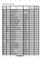
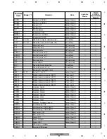
Page 58: ...U30 U31 IC 6P NC7WZ14P6X_NL SC70 6 EU AL07WZ14011 U32 IC EEPROM 8P 24LC02BT I SNG 2K SOIC EP AKE3K8B0Y50 Q26 Q28 Q33 TRAN SMD MMBT3906LT1G 40V 200MA EP BA039060013 U1 IC 16P MAX232DR SOIC EP AL000232019 IC 8P LM393DR2G SO 8 EP AL000393047 PH3 M B S S ASSY MISCELLANEOUS L1 L3 IND 560NH 230MA 5 LLQ2012 FR56J EP CV 5603JN03 L4 L6 IND SMD 10NH 5 300MA HK212510NJ T EU CVA1003JZ17 FB1 FB9 EMI FBMA 10 16...

Page 59: ... J1 J2 CONN DIP PHONE JACK 5P FR H10 LIME EP DFTJ05FR380 CON10 CON13 CONN DIP HEADER 3P 1R MS P2 0 H6 0 EP DFHD03MS673 CON14 CONN DIP HEADER 8P 1R MS P2 0 H6 0 EP DFHD08MS781 CON5 CONN DIP HEADER 9P 1R MS P2 0 H6 EP DFHD09MS441 CON9 CONN DIP HEADER 11P 1R MS P2 0 H6 EP DFHD11MS112 CON16 CONN DIP HEADER 6P 1R MS P2 5 H7 EP DFHD06MS740 CON17 CONN DIP HEADER 8P 1R MS P2 5 H7 EP DFHD08MS463 Y1 XTAL DI...

Page 60: ... HEADER 5P 1R MS P2 0 H6 6 EP DFHD05MS052 SW1 SWITCH PUSH BUTTON DIP 6P SPUN191400 EU DHP19140009 PCB BUTTON B PH3 BB ASSY MISCELLANEOUS S1 S2 S3 S4 S5 S6 SWITCH PUSH BUTTON STS 017 A EP DHPSTS01705 PH3 BUTTON B ASSY MISCELLANEOUS CN1 CONN DIP HEADER 7P 1R MR P1 25 H3 5 EP DFHD07MR0A2 PCB SENSOR B ASSY MISCELLANEOUS Q1 TRANSISTOR DIP 2N3904RLRAG TO 92 EP BAN39040D01 CON1 CONN DIP HEADER 3P 1R MS P...

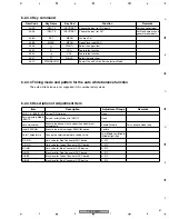
Page 61: ... enter Service mode simultaneously press the LEFT key and INPUT SET key in the system power ON state To enter Service mode simultaneously press the RIGHT key and VOL key in the system power ON state To exit the service mode AC unplugs If the servicet mode OSD is still displayed by pressing the menu button the service mode is not exited yet AC unplugs If the factory mode OSD is still displayed by p...

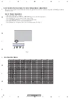
Page 62: ...ill be displayed for an instant but disappear immediately Supply signals from a PC to INPUT 1 2 If no signal is input to any input connector of the unit the system enters Burn In mode D Fig 2 D B C A Fig 1 User setting values will be reset to default initial settings 6 2 1 How to enter Factory mode To enter Service Factory mode simultaneously press the VOL key A and RIGHT key B of the unit See Fig...

Page 63: ...e At standby Input key STADBY ON POWER OFF Menu key Input key HOURMETER SIGNAL CHECK mode Burn In mode Check input source signal Auto Adjustment OSD Menu Screen auto adjust Auto White Balance ADC IC Select ADC chip Initial EEPROM Color temperature select R G B Gain and Bias set No Signal Service Factory Mode ...

Page 64: ...OL key to execute the adjustment Press the menu again to close the service factory mode 6 2 3 2 Service Menu P A H x _ 1 S _ I C J P _ 0 _ B F o a c t o d I e N P U T 1 r y M A t d j u s N O I M D x x x x x x x x x x x x x x x x x x 0 3 3 0 A u t o t m e n a l E E I n i t i M o v e t t e S i n g t e R M E N U u r n P R O M e t m p C o l o r n R G a i n G G a i n B G a i s R B i a s G B i a s B B i...

Page 65: ...e the gains and biases adjustment for R G B three Channels in ADC device Enable Disable ADC IC To select which device is selected for Auto White Balance PW3300 AD9883 Initial EEPROM Execute the initial setting of EEPROM device Yes No Color Temperature Change the color temperature setting value Low Middle Low Middle Middle High High R GAIN Gain value for Red Channel of ADC device 0 255 G GAIN Gain ...

Page 66: ...the Menu key B to open the Service factory Menu Press the RIGHT RIGHT key C to select the adjustment item Press the VOL VOL D to execute the adjustment Press the Menu key B again to close the service factory mode See Fig 4 P A H x _ 1 S _ I C J P _ 0 _ B F o a c t o d I e N P U T 2 r y M A t d j u s N O I M D x x x x x x x x x x x x x x x x x x A u t o t m e n a l E E I n i t i M o v e t t e S i n...

Page 67: ...iddle Middle High High R GAIN Gain value for Red Channel of ADC device 0 512 G GAIN Gain value for Green Channel of ADC device 0 512 B GAIN Gain value for Blue Channel of ADC device 0 512 R BIAS Black level for Red Channel of ADC device 0 512 G BIAS Black level for Green Channel of ADC device 0 512 B BIAS Black level for Blue Channel of ADC device 0 512 6 2 4 3 Key command Rem Code Key Name Key Pa...

Page 68: ...nt source to input 5 Press the input 5 key on RUC or INPUT SET A key Press the Menu key B to open the Service factory Menu Press the RIGHT RIGHT key C to select the adjustment item Press the VOL VOL D to execute the adjustment Press the Menu key B to close the service factory mode See Fig 5 P A H X _ 1 S _ I C J P _ 0 _ B F o a C t o d I e N P U T 3 r y M W a h i t e 8 3 9 8 N O I M D x x x x x x ...

Page 69: ...n Channel of ADC device 0 512 B GAIN Gain value for Blue Channel of ADC device 0 512 R BIAS Black level for Red Channel of ADC device 0 512 G BIAS Black level for Green Channel of ADC device 0 512 B BIAS Black level for Blue Channel of ADC device 0 512 Timing Mode 720 x483 59 94 Hz 483p Test Pattern SMPTE COLOR BAR 6 2 6 To leave service factory mode 6 2 5 3 Key command Rem Code Key Name Key Pad F...

Page 70: ...und Memu BHI 000 100 Adjusts the B High for color temp User Picture Menu BLW 000 100 Adjusts the B Low for color temp User Picture Menu BRT 000 100 Adjusts the brightness Picture Menu CFR 000 100 Adjusts the clock Screen Menu CLSS01 Color system AUTO Options Menu 1 CLSS02 Color system NTSC Options Menu 1 CLSS03 Color system PAL Options Menu 1 CLSS04 Color system SECAM Options Menu 1 CLSS05 Color s...

Page 71: ...en Menu IDC Clear the ID set to 0x00 t b f IDSS 00 FF Set the ID 00 FF Options Menu 1 INPS01 Switches the main screen to INPUT1 IR key input1 INPS02 Switches the main screen to INPUT2 IR key input2 INPS03 Switches the main screen to INPUT3 IR key input3 INPS04 Switches the main screen to INPUT4 IR key input 4 INPS05 Switches the main screen to INPUT5 IR key input 5 LGES01 Language English Options ...

Page 72: ...u 2 SMLS04 Side mask level 4 Options Menu 2 SOFS00 Soft focus OFF Options Menu 2 SOFS01 Soft focus 1 Options Menu 2 SOFS02 Soft focus 2 Options Menu 2 SOFS03 Soft focus 3 Options Menu 2 SOFS04 Soft focus 4 Options Menu 2 SZMS00 Sets the screen size to Dot by Dot SZMS01 Sets the screen size to 4 3 SZMS02 Sets the screen size to FULL SZMS03 Sets the screen size to ZOOM SZMS05 Sets the screen size to...

Page 73: ...0 50 28 13 74 25 Tri_level Tri_level SIGNAL V Freq Hz H Freq kHz Dot Clock MHz H Sync Polarity V Sync Polarity RGB Select DVI Standard 640 x 400 PC98 70 1 31 5 25 2 NEGA NEGA N A PC98 PC by NEC 640 x 480 VGA 59 9 31 5 25 2 NEGA NEGA N A VESA standard 72 8 37 9 31 5 NEGA NEGA N A VESA standard 75 0 37 5 31 5 NEGA NEGA N A VESA standard 85 0 43 3 36 0 NEGA NEGA N A VESA standard 848 x 480 WVGA 60 0 ...

Page 74: ...7 100 0 Sync on G Sync on G N A Mac 21 sync on G 1440 x 900 59 9 55 9 106 5 NEGA NEGA N A Apple17 1280 x 1024 EWS4800 1 60 0 64 6 1 NEGA NEGA N A EWS Work Station 1280 x 1024 EWS4800 71 2 75 1 125 0 NEGA NEGA N A EWS Work Station 1280 x 1024 HP 72 0 78 1 135 0 POSI POSI N A HP Work Station 1152 x 900 SUN 66 0 61 8 92 9 C sync C sync N A SUN C sync 76 0 71 7 105 6 C sync C sync N A SUN C sync 1280 ...

Page 75: ...s minus 1V 3 Adjustment of the 5V voltage 1 Display a color bar by means of either video signal of Video Input or composite signal input or RGB signal 2 Confirm that the voltages of TP VCC and TP GND of the power supply supply unit are maintained at 5 15 plus minus 0 1V Otherwise turn the volume control VR121 until the voltage attains 5 15 plus minus 0 1V B Adjustment of the High voltage PKG 1 Adj...

Page 76: ...ower on from power supply unit to PDP module I F Turn off the Main power supply SW and power supply ON is possible again It shutdown again if there is same symptom Green LED blinking Abnormality of FAN Motor LOCK signal of FAN Motor Failure in the fan motor Same as the description above for reference Red LED on front panel lighting No input signal When Auto Power SW control is effective Sync Separ...

Page 77: ... 35degrees 52degrees 40degrees 63degrees sensor temperature 52degrees ambience temperature 46degrees 49degrees Shutdow n point C A 5degrees Fan motor speeds change to high 50 inch 60degrees sensor temperature 40degrees ambience temperature H Sensor A H M L 48degrees 33degrees 58degrees 40degrees 71degrees 52degrees 55degrees Sensor B Shutdown point 45degrees B A View from the rear of PDP 42 inch S...

Page 78: ...level shift circuit is added to the control line from the microcomputer and the control voltage is improved Board Assy modification three of Transistor and nine of resistance additions synchronized to the mentioned board assy modifications 2 The screen becomes like white _It seems that brightness goes up when the video signal of specific VTR is input This case is generated by Y level of the Sync l...

Page 79: ...SSEMBLY 1 Remove the 9 screws 2 Remove the Stand 4 screws 4 Remove the 4 screws 3 Remove the 31 screws 5 Remove the Back Cover Back cover Rear Case section 1 x 9 x 4 x 31 Back cover 5 3 x 4 3 x 6 x 8 x 3 x 9 1 3 3 3 3 2 3 x 3 x 6 x 4 x 2 1 1 3 4 4 2 ...

Page 80: ...over Back Cover Screw 4 12 31 pcs Screw 3 6 9 pcs BACK COVER 50XM3 HANDLE 4 pcs Remove the Frame Assy and the PDP module Remove above pointed screw 16 pcs and 2 connectors After that separate Frame Assy and Front Assy Remove the connector Remove the connector Screw 4 12 16pcs Remove below pointed screws After that remove BRACKET FILTER T Remove 2 screws for holding FRONT PANEL After that remove th...

Page 81: ...0 screws 3 3 Remove the Pwr Assy 8 Remove the M B Assy 7 Remove the 6 Hexagon head screws 2 Remove the Shield cover main Assy 3 Disconnect the 4 connectors 1 Disconnect the 8 connectors 4 Remove the screw and GND terminal Input Block 3 Power Block 4 1 1 1 3 6 7 6 3 3 3 4 5 5 5 5 5 2 8 2 2 2 2 1 1 1 2 2 Pwr Assy Input Assy ...

Page 82: ... cover main Assy 1 1 1 2 Remove the 11 screws 3 Remove the 19 screws 6 Remove the 5 screws 4 Remove the screw and GND terminal 5 Disconnect the connectors Sub flme Assy Block 5 4 3 6 6 6 6 3 3 3 3 3 3 3 6 5 3 3 3 3 3 3 3 3 3 3 3 7 Remove the sub flame Assy Block 7 ...

Page 83: ...PDP 505MX 83 5 6 7 8 5 6 7 8 C D F A B E 1 2 Remove the Gasket 2 1 Remove the module Block Sub flme Assy Block Panel module Block 1 Module Block ...

Page 84: ...PDP 505MX 84 1 2 3 4 1 2 3 4 C D F A B E 1 Remove the 5 screws 2 Remove the 10 screws 3 Remove the 5 screws Front Case Assy Block 6 3 3 2 1 1 2 x 2 x 5 x 3 x 5 x 3 x 2 ...

Page 85: ...the product 1 Model Serial No and Panel ID 2 Panel Crack Exchange PDP Reconnect or exchange 4 Pixel Defect Reuse 3 Connectors Cables 5 Vertical Line 6 Horizontal Line 7 Picture Defect 8 Power off Phenomenon NG NG OK OK OK NG Reproduction Follow the procedure below for failure diagnosis Keep wearing Antistatic List Band until you finish the work ...

Page 86: ...e photographs below to find Model Serial No and Panel ID 2 Panel Crack Refer to the photographs below to check panel for crack Panel may be cracked due to handling during or after transportation Model Serial No Panel ID 222408264372 Above Example Model NP50X6MF01AA Serial No 409200160 ...

Page 87: ...f connection Caution Take care for the cable handling Careless handling in production line may cause this failure Common Voltage Flexible Cable Data Relay Flexible Cable UP Data Relay Flexible Cable Down Data Relay Board LD Digital Board High Voltage Board Common Relay Board Data Relay Board CD Data Relay Board RD Scan Relay Board D Scan Relay Board U Data Relay Board LU Common Connection Board Da...

Page 88: ...elay Board Photo Panel Right Connection Part 2 Locked Unlocked Digital Board Photo High Voltage Board High Voltage Board Photo Data Relay Board High Voltage Board Photo Scan Relay Board Photo Right Connection Part 3 Locked Unlocked Data Relay Board Photo Panel Common Connection Board Photo Common Relay Board High Voltage Board Photo Common Relay Board Photo ...

Page 89: ...fect Refer to the below for diagnosis Symptom Bright defect or dark defect Cause Countermeasure PDP failure if out of spec Exchange PDP Note Typical Symptom are only shown Another Symptom might appear 1 pixel 2 pixels 2 pixels 3 pixels 3 pixels 3 pixels ...

Page 90: ...ttern Normal All Blue Pattern Red 1 Line All Black Pattern Normal All Green Pattern Red 1 Line All Blue Pattern Red 1 Line All Black Pattern Normal Cause Countermeasure 1 Failure in Data IC Exchange PDP 2 Failure in panel Exchange PDP Cause Countermeasure 1 Open or contact failure of Data flexible cable Clean Reconnect or exchange connector 2 Failure in Data IC Exchange PDP Cause Countermeasure 1 ...

Page 91: ...an Relay Board side Clean Reconnect or exchange connector 3 Contact failure of connector between Scan Board and Scan Relay Board Clean Reconnect or exchange connector 4 Short between terminals of Scan IC due to screw dust Clean around the terminals 7 Picture Defect 7 1 Symptom No Picture Priming flash Note Typical symptom are only shown Another Symptom might appear High Voltage Board Glass Fuse F3...

Page 92: ...y Board CU is short circuited between Pin 2 and GND Pin 3 or 4 Data Relay Board CU is failed Exchange Data Relay Board CU Data Relay Board LD Data Relay Board CD Data Relay Board RD Data Relay Board RD CN8 CN1 CN8 CN3 CN3 OK Open NG Short Cause Countermeasure 6 If the connector CN8 disconnected from Data Relay Board RD is short circuited between Pin 5 or 6 and GND Pin 3 or 4 Data IC is broken Exch...

Page 93: ...4 P 76 78 O 71 74 N 66 69 M 61 64 L 57 59 K B 6 9 C 10 13 D 15 18 E 24 F 33 35 G 39 40 H 49 50 I 53 J 55 56 OK Diode characteristic NG Other than above 7 2 Symptom No Picture Priming doesn t flash if W X terminals doesn t have Diode characteristic Cause Countermeasure No Diode characteristic Exchange High Voltage Board 7 3 Symptom No Picture Priming doesn t flash Cause Countermeasure R146 open Exc...

Page 94: ...ngular color shear color discrepancy shear in display Out of synchronization or duplication Mosaic One or more vertical bands Multiple vertical lines Cause Countermeasure 1 Contact failure of connector adjacent to Digital Board or short circuit due to conductive obstacle Clean or Reconnect 2 Failure in circuit on Digital Board Failure in Digital Board ...

Page 95: ...ymptom are only shown Another Symptom might appear Chip Fuse FU801 Glass Fuse F301 F1 Digital Board High Voltage Board High Voltage Board OK Short NG Open OK Short NG Open OK Short NG Open Cause Countermeasure 1 F301 open Exchange High Voltage Board 2 FU801 open Exchange Digital Board 3 F1 open Exchange High Voltage Board ...

Page 96: ... Short Cause Countermeasure If short circuited disconnect connector between High Voltage Board and Scan Relay Board and 4 Short between NEGA POSI on High Voltage Board Exchange High Voltage Board 5 Short between NEGA POSI on Scan Relay Board U Exchange Scan Relay Board U 6 Short between NEGA POSI on Scan Relay Board D Exchange Scan Relay Board D High Voltage Board High Voltage Board ...

Page 97: ...05MX 97 5 6 7 8 5 6 7 8 C D F A B E 8 2 Symptom No Picture Power off Priming flash Fuse Resistor R91 R91 OK About 2 2Ω 1W NG Open Cause Countermeasure R91 open Exchange High Voltage Board High Voltage Board ...

Page 98: ...61 R43 OK About 3 3Ω 2W NG Open R61 OK About 4 7Ω 2W NG Open R150 OK About 4 7Ω 2W NG Open Cause Countermeasure R43 R61 open Exchange High Voltage Board 8 4 Symptom White Pattern even in no signal Power off Cause Countermeasure R150 open Exchange High Voltage Board Dark and rough picture Many light spots on dark portion ...

Page 99: ...nel 1 Disconnect connectors and cables on failed Board 2 Detach failed Board 2 Put on good Board 3 Connect connectors and cables Follow the procedure below for diagnosis Procedure Caution Put cushion under failed PDP to cover general surface of glass before laying it s screen down ...

Page 100: ...and connectors to avoid failure Be sure to take off Heat Sink before detach Data Relay Board See next Page for the procedure 2 Loosen screws of failed Board and put on good Board Data Relay Board LU 3 screws Common Relay Board 15 screws Digital Board 4 screws High Voltage Board 15 screws Common Connection Board 9 screws Scan Relay Board U 2 screws Scan Relay Board D 2 screws Scan Relay Connection ...

Page 101: ...Sink heat conductive silicone sheet See Photo 4 Before detaching Heat Sink Heat Sink and Data TCP Repeat 1 2 3 4 1 Slowly swing Heat Sink back and forth 1 2 2 Gently lift Heat Sink up from Data TCP 1 2 3 Repeat 1 and 2 until Heat Sink is taken off 3 Reverse of Heat Sink Heat conductive silicone sheet Data TCP mounted On flexible cable Be careful of sticking ...

Page 102: ...ctors Common Connection Board 7 connectors Scan Relay Board U 5 connectors Scan Relay Board D 5 connectors Data Relay Board CU 11 connectors Data Relay Board RU 8 connectors Data Relay Board LD 6 connectors Data Relay Board CD 11 connectors Data Relay Board RD 8 connectors Caution Be sure to put on Heat Sink after assembling Data Relay Board Common Relay Board 2 connectors ...

Page 103: ... Inspection Voltage Adjust Aging Display Inspection Trouble Shooting Reuse next process Detach PDP from Jig Keep it if PDP is assembled Into product set Caution Be sure to connect a Signal Cable and two Power Cables Otherwise High Voltage Board may be broken OK NG Example of mounting to jig ...

Page 104: ...irm voltages on Voltage label before conducting adjustment 3 Adjustment of Vsw1 Vsw2 Caution Use the nearest chassis for grounding Vsw1 Adjust VR3 so that the voltage between Test Pad TP328 and GND becomes Rated Voltage on Label 0 5V Vsw2 Adjust VR4 so that the voltage between Test Pad TP310 and GND becomes Rated Voltage on Label 0 5V Example Vbw 119 9 Vsw1 220 3 Vp 224 6 Vsw2 215 0 s195 0 d70 0 1...

Page 105: ...earest chassis for grounding Vp Adjust VR1 so that the voltage between Test Pad TP327 and GND becomes Rated Voltage on Label 0 5V Vbw Adjust VR2 so that the voltage between Test Pad TP329 and GND becomes Rated Voltage on Label 0 5V High Voltage Board TP327 Vp TP329 Vbw VR2 Vbw VR1 Vp ...

Page 106: ...minutes Caution Do not use a fixed pattern such as window or cross hatch for aging White Red Green Blue Color Bars Gray Scale 6 Display Inspection Confirm that every signal picture is good Caution PDP module may have instable picture display if electrified after a long storage Then conduct aging for about 2 hours ...

Page 107: ...ce 10 INPUT 5 COMPONENT Direct access of input 5 YUV source 11 MENU Displays the menus screen Leave the menus screen 12 UP ARROW Navigate up in the OSM 13 LEFT ARROW Navigate left in the OSM 14 RIGHT ARROW Navigate right in the OSM 15 DOWN ARROW Navigate down in the OSM 16 SET Accept the selected item in the OSM Change the setting value of selected item which don t has the sub menu Return to the p...

Reviews: