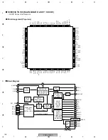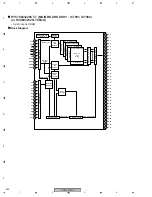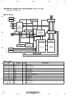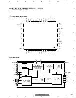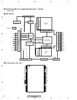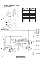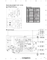
PDP-5050SX
204
1
2
3
4
1
2
3
4
C
D
F
A
B
E
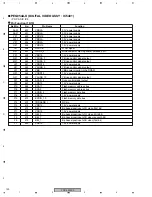
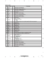
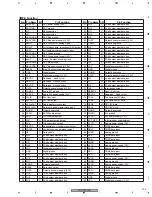
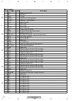
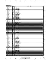
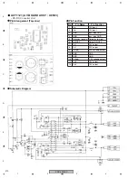
No.
Pin Name
I/O
Pin Function
1
VCC
−
Digital power supply (3.3V)
2
DE
I
Data enable
3
VREF
I
3.3V fixed
4
HSYNC
I
Horizontal sync. control signal input
5
VSYNC
I
Vertical sync. control signal input
6
CTL3
I
External CTL3 input
7
NC
−
No connection
8
NC
−
No connection
9
HTPLG
I
Monitor chrage input
10
PD#
I
Power down input (Active low)
11
MSEN
O
Monitor sense output (open-collector output)
12
VCC
−
Digital power supply (3.3V)
13
ISEL/RST#
I
I2C interface selecting input High: I2C interface is active
14
SDAS
I/O
DDC I2C data input/output
15
SCLS
I
DDC I2C clock input
16
GND
−
Digital ground
17
PGND1
−
PLL analog ground
18
PVCC1
−
Analog power supply for PLL of primary side (3.3V)
19
EXT_SWING
I
Voltage regulation adjustment
20
AGND
−
Analog ground
21
TXC-
O
Differential signal clock output of TMDS Low voltage
22
TXC+
O
Differential signal clock output of TMDS Low voltage
23
AVCC
−
Analog power supply (3.3V)
24
TX0-
O
Differential signal clock output of TMDS Low voltage
25
TX0+
O
Differential signal clock output of TMDS Low voltage
26
AGND
−
Analog ground
27
TX1-
O
Differential signal clock output of TMDS Low voltage
28
TX1+
O
Differential signal clock output of TMDS Low voltage
29
AVCC
−
Analog power supply (3.3V)
30
TX2-
O
Differential signal clock output of TMDS Low voltage
31
TX2+
O
Differential signal clock output of TMDS Low voltage
32
AGND
−
Analog ground
33
VCC
−
Digital power supply (3.3V)
34
RESERVED
I
Reserved pin for Silicon Image Normally, fixed to low.
35
GND
−
Digital ground
36
D23
I
24-bit pixel bus input
37
D22
I
24-bit pixel bus input
38
D21
I
24-bit pixel bus input
39
D20
I
24-bit pixel bus input
40
D19
I
24-bit pixel bus input
41
D18
I
24-bit pixel bus input
42
D17
I
24-bit pixel bus input
43
D16
I
24-bit pixel bus input
44
D15
I
24-bit pixel bus input
45
D14
I
24-bit pixel bus input
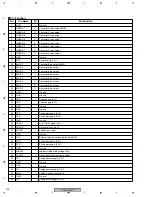
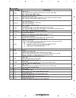
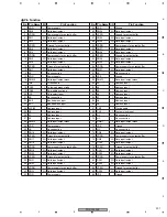
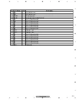
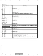
Pin Function

