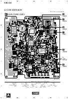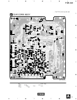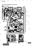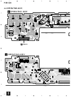
PDR-509
37
A
B
C
D
1
2
3
4
1
2
3
4
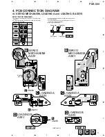
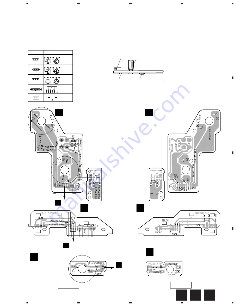
4. PCB CONNECTION DIAGRAM
4.1 SERVO MECHANISM, LOADING A and LOADING B ASSYS
D
C
B
NOTE FOR PCB DIAGRAMS :
1. Part numbers in PCB diagrams match those in the schematic
diagrams.
2. A comparison between the main parts of PCB and schematic
diagrams is shown below.
3. The parts mounted on this PCB include all necessary parts for
several destinations.
For further information for respective destinations, be sure to
check with the schematic diagram.
4. View point of PCB diagrams.
Symbol In PCB
Diagrams
Symbol In Schematic
Diagrams
Part Name
B C E
D
D
G
G
S
S
B C E
B
C
E
D
G
S
B
C
E B
C
E
B
C
E
Transistor
Transistor
with resistor
Field effect
transistor
Resistor array
3-terminal
regulator
Capacitor
Connector
P.C.Board
Chip Part
SIDE A
SIDE B
SIDE A
SIDE B
(PNP1447-C)
CN452
A
CN451
A
CN453
A
SERVO
MECHANISM
ASSY
B
LOADING A
ASSY
C
LOADING B
ASSY
D
LOADING B
ASSY
D
LOADING A
ASSY
C
SERVO
MECHANISM
ASSY
B
M
M
M
CARRIAGE
MOTOR
SPINDLE
MOTOR
LOADING
MOTOR
Summary of Contents for PDR-509
Page 19: ...PDR 509 19 A B C D 5 6 7 8 5 6 7 8 CDR SERVO AMP MULTI PLEXER A1 5 A4 5 A3 5 A1 5 1 3 5 A ...
Page 43: ...PDR 509 43 A B C D 5 6 7 8 5 6 7 8 PNP1466 A Q701 Q704 PNP1466 A CN51 J SIDE A SIDE B I ...
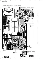
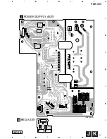
Page 45: ...PDR 509 45 A B C D 1 2 3 4 1 2 3 4 J K PNP1466 A POWER SUPPLY ASSY J REG ASSY K SIDE B ...
Page 68: ...68 PDR 509 FL TUBE 7 2 2 DISPLAY PEL1099 FUNCTION ASSY V701 Anode Grid Assignment 1 35 ...
Page 69: ...69 PDR 509 Pin Assignment ...
Page 73: ...73 PDR 509 MONITOR DIGITAL REC LEVEL ANALOG REC LEVEL INPUT SELECTOR TIME REPEAT ...

