background image

55

PDR-509

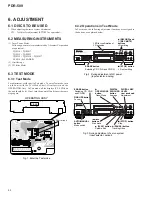
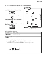
6.5 ADJUSTMENT 2 (SERVO SYSTEM ADJUSTMENT)

[Procedure]

(1) Press the AUTO/MANUAL button until "01 F4" appears on the FL display.

(2) Adjust with the DIGITAL REC LEVEL knob until the value for Pin 6 of CN102 is 0 mV 

±

 10 mV.

(3) Press the DIGITAL REC LEVEL knob to register the adjustment.

Once the adjustment is registered with the DIGITAL REC LEVEL knob, "?" on the FL display will disappear.

6.5.1 Focus Offset Adjustment

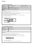
CN102 - pin 6 (FE)

Test Point

Adjustment Point

Adjustment Value

0 mV 

±

 10 mV

Oscilloscope

10:1 probe

10 : 1

FE

VC

DIGITAL REC LEVEL knob

For servo adjustment, set the INPUT SELECTOR to OPTICAL.

Use the DIGITAL REC LEVEL Knob to make the adjustments.

To reset the adjusted values to the initial settings, press and hold the
MONITOR button for 4 seconds.

To register an adjustment, press the DIGITAL REC LEVEL Knob.

Fig. 6 Adjustment points

CN102

1

1 : RF
2 : VC
3 : MPP
4 : TE
5 : VC
6 : FE

6

CD-R CORE ASSY

DIGITAL

REC LEVEL

DIGITAL

REC LEVEL

MONITOR

INPUT

SELECTOR

MONITOR

INPUT

SELECTOR

Symptom when out of
adjustment

The model does not focus-in

Summary of Contents for PDR-509

Page 1: ... TROUBLE SHOOTING 58 7 1 2 DISASSEMBLY 59 7 1 3 DIAGNOSIS OF CD R CORE ASSY 61 7 2 PARTS 62 7 2 1 IC 62 7 2 2 DISPLAY 68 7 3 EXPLANATION 70 7 3 1 ERROR CODE 70 8 PANEL FACILITIES AND SPECIFICATIONS 72 T IZE AUG 1999 Printed in Japan COMPACT DISC RECORDER Type Model Power Requirement Remarks PDR 509 KU CA AC120V MY AC220 230V MV AC220 230V THIS MANUAL IS APPLICABLE TO THE FOLLOWING MODEL S AND TYPE...

Page 2: ... evident from visual inspection nor the protection afforded by them necessarily can be obtained by using replacement components rated for voltage wattage etc Replacement parts which have these special safety characteristics are identified in this Service Manual Electrical components having such features are identified by marking with a on the schematics and on the parts list in this Service Manual...

Page 3: ...lso does not function in the test mode Laser diode oscillation will continue if pin 1 of M51593FP IC101 on the PRE AMP BOARD ASSY mounted on the CD R PICKUP is connected to GND or pin 19 is connected to low level ON or else the terminals of Q101 are shorted to each other fault condition 2 When the cover is opened with the servo mechanism block removed and turned over close viewing of the objective...

Page 4: ...Unit PWW1163 CU PD114 6 Battery Cover RZN1156 NSP 7 Dry Cell Battery R6P AA VEM 013 8 Polyethylene Bag Z21 038 0 03 230 340 9 Packing Case See Contrast table 2 10 Protector F RHA1238 11 Protector R RHA1239 12 Mirror Mat Sheet Z23 007 13 Operating Instructions See Contrast table 2 Dutch Swedish Spanish Danish 14 Operating Instructions See Contrast table 2 English French German Italian 15 Rear Space...

Page 5: ...ANEL SECTION H G E E B K J A D C F G I H B D C A KU CA Type Only KU CA Type Only F I J K 24 24 22 17 15 13 13 13 24 24 20 28 34 6 27 36 19 22 34 34 31 32 1 27 22 22 22 22 22 9 25 25 25 4 3 2 5 22 22 16 14 24 24 24 29 30 22 11 35 24 24 24 18 MY Type Only MY Type Only MV Type Only 22 26 23 23 7 22 34 33 12 10 ...

Page 6: ...on Label See Contrast table 2 29 Caution Label HE See Contrast table 2 30 Caution Label See Contrast table 2 NSP 31 Mecha Base PNB1613 32 Radiation Sheet PEB1305 33 PCB Spacer AEC1371 34 Screw BBZ30P080FCC 35 Caution Label See Contrast table 2 36 Disc Caution Label See Contrast table 2 Mark No Symbol and Description Part No Remarks KU CA Type MY Type MV Type NSP 2 3 4 5 7 16 16 28 29 30 35 36 AUDI...

Page 7: ...C2204 13 Sub Panel PNW2797 14 Function Lens PNW2796 15 Headphone Knob PAC1707 16 Name Plate PAM1776 17 VOL Knob L PAC1902 18 VOL Knob R PAC1903 19 JOG Knob B RAC2210 20 Screw PPZ30P100FMC 21 Screw ABA1005 22 Getter Label See Contrast table 2 23 CD R Getter PRW1547 24 19P Flexible Cable 60V PDD1196 Mark No Symbol and Description Part No Remarks KU CA Type MY Type MV Type 3 4 4 5 22 22 OPERATING Ass...

Page 8: ...1634 7 Screw VBA1055 8 Tray Stopper Spring VBH1277 9 Rubber Belt VEB1260 10 Loading Base VNL1844 11 Tray VNL1731 12 Gear Pulley VNL1733 13 Loading Gear VNL1734 14 Drive Gear VNL1735 15 Drive Cam VNL1736 16 Lock Plate VNL1820 17 Tray Stopper VNL1739 18 Connector Assy PF03KK E37 LOADING A CN501 CD R CORE CN451 19 Screw BBZ26P040FMC 20 Screw IPZ20P080FMC 21 Loading Motor Assy VXX2505 22 Binder PEC 10...

Page 9: ... Disc Table PNW2860 16 Carriage Base S PNW2874 17 Connector Assy PG09KK E17 SERVO MECHANISM CN601 CD R CORE CN452 18 Guide Bar VLL1488 19 Sub Guide Bar VLL1489 NSP 20 Magnet VYM1024 21 CD R Pickup PEA1351 22 Screw IPZ20P060FMC 23 Screw PMZ20P030FMC 24 Screw JGZ17P030FMC 25 Disc Table Assy PEA1349 26 Carriage Motor Assy PEA1350 Use nippers or other tool to cut the two sections marked A in figure 1 ...

Page 10: ... STRATEGY CONTROL IC IC451 M56788FP TRK DRIVER FCS DRIVER SLD DRIVER SPDL DRIVER LOADING DRIVER Disc CD CD R CD RW 10 9 16 15 17 8 14 11 4 1 3 2 4 1 3 6 1 76 34 19 58 43 65 39 41 50 4 6 73 2 10 9 16 15 17 8 14 B C D E F G H FCS FCS FCS TRK TRK FG SPDL 11 A B C D 11 29 38 19 TE TE AD0 AD7 Address HF 10 RFAC FE TE RFAC 29 RFWBL RFWBL 46 E F G H SERVO MECHANISM ASSY B CD R CORE ASSY A 9 3 4 M CARRIAG...

Page 11: ...5110B MODE CONTROL MICROCOMPUTER D704 MODE DISPLAY LED D701 D702 V701 PEL1099 FL DISPLAY KEY MATRIX IC702 S 806E RESET IC PHONES IC401 KU CA PCM1716E MY MV PE8001A DA CONVERTER IC404 IC406 IC651 IC651 OUTPUT L ch R ch 16 9344MHz AD0 AD7 Address Address Data AUDIO ASSY E AUDIO ASSY E HEADPHONE ASSY F VR ASSY G DIGITAL I O ASSY H OPERATING ASSY I 43 36 61 60 59 3 2 4 43 17 22 18 19 3 15 16 17 CDLRCK...

Page 12: ... MY MV PWZ4009 J REG ASSY KU CA PWZ4012 MY MV PWZ4013 K OPERATING ASSY KU CA PWZ3977 MY MV PWZ3978 I DIGITAL I O ASSY KU CA PWZ4020 MY MV PWZ4021 H AC POWER CORD KU CA ADG7021 MY ADG1127 MV ADG7004 KU CA 120V MY MV AC220 230V COAXIAL COAXIAL OPTICAL DIGITAL OUT OPTICAL CN1 KU CA AKP1122 MY MV AKP7005 T1 POWER TRANSFORMER KU CA PTT1356 MY MV PTT1357 DIGITAL IN CN453 CN101 CN451 CN452 J31 J651 J22 J...

Page 13: ... 1 2 E 2 2 AUDIO ASSY KU CA PWZ3996 MY MV PWZ3997 E HEADPHONE ASSY PWZ3988 F VR ASSY PWZ3992 G L R LINE IN CONTROL IN L R LINE IOUT J403 Note When ordering service parts be sure to refer to EXPLODED VIEWS and PARTS LIST or PCB PARTS LIST ...

Page 14: ...PDR 509 14 A B C D 1 2 3 4 1 2 3 4 A 1 5 CD R CORE ASSY PYY1273 MECHA CONTROL µCOM BLOCK A5 5 A2 5 A3 5 ATIP DECODER 3 3 CD R CORE ASSY 1 5 1 5 A ...

Page 15: ...PDR 509 15 A B C D 5 6 7 8 5 6 7 8 A4 5 CN804 E 2 2 L302 L305 L309 L311 L315 L318 L319 OTL1040 IC303 PYY1196 BR93LC46F EEPROM MECHA µ COM 8 bit LATCH CN301 8 9 10 11 12 1 2 3 4 5 6 7 1 5 A ...

Page 16: ...DR 509 16 A B C D 1 2 3 4 1 2 3 4 A 2 5 CD R CORE ASSY PYY1273 CD R PICKUP PEA1351 RF PROCESSOR BLOCK MULTI PLEXER MULTI PLEXER CN1 CN101 7 8 R R R R R R R R 3 4 CD R CORE ASSY 2 5 and CD R PICKUP 2 5 A ...

Page 17: ...PDR 509 17 A B C D 5 6 7 8 5 6 7 8 A3 5 A3 5 A1 5 A4 5 A5 5 RF PROCESSOR CN102 4 3 2 1 5 6 R RF SIGNAL ROUTE R R R R R R AUDIO SIGNAL ROUTE REC 2 5 A ...

Page 18: ...PDR 509 18 A B C D 1 2 3 4 1 2 3 4 A 3 5 CD R CORE ASSY PYY1273 SERVO BLOCK A2 5 A1 5 A5 5 A2 5 2 3 5 CD R CORE ASSY 3 5 3 5 A ...

Page 19: ...PDR 509 19 A B C D 5 6 7 8 5 6 7 8 CDR SERVO AMP MULTI PLEXER A1 5 A4 5 A3 5 A1 5 1 3 5 A ...

Page 20: ...PDR 509 20 A B C D 1 2 3 4 1 2 3 4 A 4 5 CD R CORE ASSY PYY1273 DIGITAL BLOCK A3 5 A2 5 A1 5 EFM ENCODER IC D RA VCO STRATEGY CONTROL 17 18 16 14 15 13 R R R R R R R R R R 3 6 CD R CORE ASSY 4 5 4 5 A ...

Page 21: ... L511 L513 L515 L518 L522 L524 L526 OTL1040 F510 F514 F520 F521 F527 VTH1097 16 9344MHz MULTI PLEXER FS CONVERTER D RAM VCO 2 3 1 4 6 7 8 9 10 11 5 12 R AUDIO SIGNAL ROUTE R R R R R R AUDIO SIGNAL ROUTE REC The power supply is shown with the marked box 4 5 A ...

Page 22: ...ECHANISM ASSY PWZ3759 B LOADING B ASSY PWZ3761 D LOADING A ASSY PWZ3760 C PC651 NJL5803K F1 CARRIAGE MOTOR ASSY SLIDER PEA1350 LOADING MOTOR ASSY VXX2505 DC MOTOR ASSY SPINDLE PEA1235 J601 CN601 CN551 CN501 CN452 CN451 CN453 S601 S501 3 1 2 3 7 CD R CORE 5 5 SERVO MECHANISM LOADING A and LOADING B ASSYS 5 5 A B C D ...

Page 23: ...PDR 509 23 A B C D 5 6 7 8 5 6 7 8 A1 5 A4 5 A2 5 CN21 J CD DECODER CN901 5 4 RF SIGNAL ROUTE AUDIO SIGNAL ROUTE The power supply is shown with the marked box 5 5 A ...

Page 24: ... BLOCK J31 J J651 H CN402 CN801 CN802 CN401 E 2 2 E 2 2 E 2 2 E 2 2 E 2 2 E 2 2 D A CONVERTER KU CA PCM1716E MY MV PEB8001A KU CA PCH1141 MY MV PCH1122 CN501 A4 5 PS80503 PS80503 PS80503 PS80503 PS80503 PS80503 PS80503 PS80503 R2898 0 R PS80503 1 2 E 3 8 AUDIO 1 2 and HEADPHONE ASSYS ...

Page 25: ...KU CA PCH1142 MY MV PCH1126 KU CA PCH1142 MY MV PCH1128 PCH1127 R413 R416 RN1 10SE KU CA 4700pF MY MV 1500pF KU CA 4700pF MY MV 1500pF KU CA PCH1142 MY MV PCH1126 KU CA PCH1142 MY MV PCH1126 KU CA PCH1142 MY MV PCH1126 PS80503 PS80503 J3 J D20PYY0310E QTL1015 QTL1015 QTL1015 R AUDIO SIGNAL ROUTE AUDIO SIGNAL ROUTE REC The power supply is shown with the marked box F 1 2 E ...

Page 26: ... PWZ3996 MY MV PWZ3997 A D BLOCK LINE IN LINE IN JA801 1 2 JA801 2 2 CN806 J851 CN803 ANALOG REC VOLUME VR ASSY PWZ3992 G The power supply is shown with the marked box R AUDIO SIGNAL ROUTE REC R R R R R R R R R R R R R R R R 3 9 AUDIO 2 2 and VR ASSYS 2 2 E G ...

Page 27: ...PDR 509 27 A B C D 5 6 7 8 5 6 7 8 CN804 VKN1246 CN805 CN701 CN301 I E 1 2 E 1 2 E 1 2 E 1 2 E 1 2 E 1 2 A1 5 E 1 2 R R R R R 2 2 E ...

Page 28: ...PDR 509 28 A B C D 1 2 3 4 1 2 3 4 DIGITAL OUT DIGITAL IN DIGITAL IN JA652 DIGITAL OUT JA654 JA653 JA651 KU CA PCH1143 MY MV 100 50 H 3 10 DIGITAL I O ASSY ...

Page 29: ...PDR 509 29 A B C D 5 6 7 8 5 6 7 8 DIGITAL I O ASSY KU CA PWZ4020 MY MV PWZ4021 H J651 D20PYY0605E CN802 E 1 2 The power supply is shown with the marked box H ...

Page 30: ...PDR 509 30 A B C D 1 2 3 4 1 2 3 4 OPERATING ASSY KU CA PWZ3977 MY MV PWZ3978 I J701 51048 0600 CN51 J FL HOLDER 100 10 0 1 KU CA ONLY MY MV ONLY 3 11 OPERATING ASSY I ...

Page 31: ...PDR 509 31 A B C D 5 6 7 8 5 6 7 8 CN701 CN805 E 2 2 MY MV ONLY KU CA ONLY The power supply is shown with the marked box MODE CONTROLLER SYSTEM RESET J703 J703 J703A 51048 0300 51048 0300 D20PYY0315E I ...

Page 32: ...pF MY MV 1000pF 3 5A CAUTION FOR CONTINUED PROTECTION AGAINST RISK OF FIRE REPLACE ONLY WITH SAME TYPE NO ICP N10 MFD BY ROHM CO LTD FOR IC35 AND IC36 CAUTION FOR CONTINUED PROTECTION AGAINST RISK OF FIRE REPLACE ONLY WITH SAME TYPE NO ICP N15 MFD BY ROHM CO LTD FOR IC22 IC23 AND IC25 CAUTION FOR CONTINUED PROTECTION AGAINST RISK OF FIRE REPLACE ONLY WITH SAME TYPE NO 49103 5 MFD BY LITTELFUSE INC...

Page 33: ...CA PWZ4012 MY MV PWZ4013 K CN11 CN21 J31 CN51 CN901 A5 5 CN402 E 1 2 GNDSN E 1 2 KU CA PDF1201 MY MV PDF1199 J3 B6B PH K S J701 I KU CA 100 35 MY MV 220 35 KU CA 0 01 MY MV 0 027 KU CA 0 01 MY MV 0 027 MY MV ONLY MY MV ONLY KU CA ONLY MY MV ONLY K J ...

Page 34: ... 0V 5V at MUTE ON Audio Signal Not Output at MUTE OFF Audio Signal Output AMUTE CN501 pin9 5V 0V LRSTD CN501 pin10 5V Note The encircled numbers denote measuring point in the schematic diagram 1 CN301 pin 5 MREQ V 0 2V div 10 1 H 5msec div STOP 2 CN301 pin 6 EN_CE V 0 2V div 10 1 H 5msec div STOP 3 CN301 pin 8 XFUSE V 0 2V div 10 1 H 5msec div STOP 4 CN301 pin 9 MACK V 0 2V div 10 1 H 5msec div ST...

Page 35: ... pin 6 FE V 5mV div 10 1 H 2msec div PLAY 5 TP113 RFAC V 0 2V div 10 1 H 0 2µsec div PLAY 6 IC101 pin 22 ATFG V 0 2V div H 20µsec div REC 7 CN101 pin 3 TRK V 0 2V div 10 1 H 5msec div STOP 8 CN101 pin 4 FCS V 0 2V div 10 1 H 5msec div STOP CD R CORE ASSY A2 5 CD R CORE ASSY A3 5 1 TP210 FG V 0 2V div 10 1 H 1msec div PLAY 2 Foot of R212 SPDL V 20mV div H 2msec div PLAY ...

Page 36: ... V 0 2V div 10 1 H 50msec div REC 15 IC431 pin 25 ODON V 0 2V div 10 1 H 0 1µsec div REC 16 IC431 pin 29 WLDON V 0 2V div 10 1 H 1msec div REC 17 IC431 pin 34 REWLDON V 0 2V div 10 1 H 1msec div REC 5 CN501 pin 12 CL V 0 2V div 10 1 H 0 5µsec div STOP 11 CN501 pin 20 DIN2 V 0 2V div 10 1 H 0 2µsec div REC_Coaxial 18 TP503 W XR V 0 2V div 10 1 H 1msec div REC 1 CN452 pin 2 SL V 0 2V div 10 1 H 5mse...

Page 37: ...information for respective destinations be sure to check with the schematic diagram 4 View point of PCB diagrams Symbol In PCB Diagrams Symbol In Schematic Diagrams Part Name B C E D D G G S S B C E B C E D G S B C E B C E B C E Transistor Transistor with resistor Field effect transistor Resistor array 3 terminal regulator Capacitor Connector P C Board Chip Part SIDE A SIDE B SIDE A SIDE B PNP1447...

Page 38: ...933 IC351 IC371 IC301 IC304 IC503 Q301 Q302 Q303 Q402 Q401 IC401 IC501 IC507 IC506 IC352 IC451 IC201 IC502 IC509 Q203 Q203 IC251 IC254 Q201 IC101 Q142 IC562 IC431 VR161 VR141 VR162 VR163 VR101 CN21 J CD R CORE ASSY A CN804 E CN801 E To CD R PICKUP CN601 B CN501 C CN551 D SIDE A This PCB is a four layered board ...

Page 39: ...PDR 509 39 A B C D 1 2 3 4 1 2 3 4 A PNP1465 B Q551 Q202 IC255 IC505 IC508 IC181 Q102 IC561 IC141 IC161 Q103 Q141 CD R CORE ASSY A SIDE B This PCB is a four layered board ...

Page 40: ...3 4 1 2 3 4 4 3 AUDIO HEADPHONE and VR ASSYS E F G Q405 Q408 Q401 IC404 IC402 Q801 Q402 IC401 IC451 IC801 IC802 IC803 PNP1466 A PNP1466 A PNP1466 A J31 J AUDIO ASSY E VR ASSY G HEADPHONE ASSY F CN501 A CN301 A CN701 I SIDE A ...

Page 41: ...PDR 509 41 A B C D 1 2 3 4 1 2 3 4 E F G Q409 Q404 IC406 Q403 PNP1466 A PNP1466 A PNP1466 A AUDIO ASSY E VR ASSY G HEADPHONE ASSY F SIDE B ...

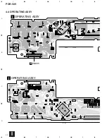
Page 42: ...PDR 509 42 A B C D 1 2 3 4 1 2 3 4 Q705 IC701 IC702 CN805 E OPERATING ASSY I OPERATING ASSY I 4 4 OPERATING ASSY I ...

Page 43: ...PDR 509 43 A B C D 5 6 7 8 5 6 7 8 PNP1466 A Q701 Q704 PNP1466 A CN51 J SIDE A SIDE B I ...

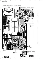
Page 44: ... A B C D 1 2 3 4 1 2 3 4 4 5 POWER SUPPLY and REG ASSYS J K PNP1466 A IC33 IC31 IC35 IC32 IC36 IC1 IC25 IC23 IC22 IC24 IC21 CN901 A J701 I CN402 E T1 POWER TRANSFORMER AC IN POWER SUPPLY ASSY J REG ASSY K SIDE A ...

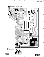
Page 45: ...PDR 509 45 A B C D 1 2 3 4 1 2 3 4 J K PNP1466 A POWER SUPPLY ASSY J REG ASSY K SIDE B ...

Page 46: ...PDR 509 46 A B C D 1 2 3 4 1 2 3 4 4 6 DIGITAL I O ASSY H 150 IC651 IC652 Q651 PNP1466 A PNP1466 A CN802 E DIGITAL I O ASSY H DIGITAL I O ASSY H SIDE A SIDE B ...

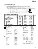
Page 47: ...R SUPPLY ASSY REG ASSY PYY1273 PWX1570 PWZ3759 PWZ3760 PWZ3761 PWM2282 PWZ3996 PWZ3988 PWZ3992 PWZ4020 PWZ3977 PWZ4008 PWZ4012 PYY1273 PWX1570 PWZ3759 PWZ3760 PWZ3761 PWM2283 PWZ3997 PWZ3988 PWZ3992 PWZ4021 PWZ3978 PWZ4009 PWZ4013 PYY1273 PWX1570 PWZ3759 PWZ3760 PWZ3761 PWM2283 PWZ3997 PWZ3988 PWZ3992 PWZ4021 PWZ3978 PWZ4009 PWZ4013 CD R CORE ASSY SEMICONDUCTORS IC502 AD1893JST IC101 AK8563 IC321 ...

Page 48: ... CKSQYB272K50 C104 C221 CKSQYB331K50 C103 CKSQYB333K50 C131 C215 C227 C229 CKSQYB334K16 C128 C134 C363 C474 C475 CKSQYB471K50 C206 C413 CKSQYB473K25 C102 CKSQYB473K50 C119 C204 C468 C469 CKSQYB681K50 C463 C464 CKSQYB682K50 C205 CKSQYB823K25 C133 C153 C254 C303 C322 CKSQYF103Z50 C362 C416 C433 C519 CKSQYF103Z50 C521 C522 C555 C561 C562 CKSQYF103Z50 C568 C569 C905 CKSQYF103Z50 C106 C108 C111 C120 C1...

Page 49: ...411 C412 C809 C811 220µF 25V PCH1142 RESISTORS R440 RD1 2VM272J R475 R476 RD1 4VM102J R427 R428 RD1 4VM223J R429 R432 RD1 4VM471J R411 R412 RDR1 2PM101J R413 R414 RN1 10SE1002D R415 R416 RN1 10SE1202D R807 R808 RS1 2LMF101J R441 RS1LMF272J Other Resistors RS1 10S J OTHERS CN401 3P JUMPER CONNECTOR 52147 0310 CN802 6P JUMPER CONNECTOR 52147 0610 CN402 8P JUMPER CONNECTOR 52147 0810 CN805 19P FFC CO...

Page 50: ...R 51048 0600 J651 JUMPER WIRE 6P D20PYY0605E JA653 OPTICAL LINK OUT GP1F32T JA651 OPTICAL RECEIVE MOD GP1F37R JA654 1P JACK ORG PKB1028 JA652 1P JACK ORG PKB1033 PCB BINDER VEF1040 SEMICONDUCTORS IC701 PE5110B IC702 S 806E Q705 2SC2412K Q701 Q703 DTA124EK D701 D702 D704 SLR 343VC NPQ SWITCHES S701 RSC1003 S702 S719 VSG1009 CAPACITORS C701 CCSQCH101J50 C739 CEAT101M10 C702 C781 C782 CKSQYB103K50 C7...

Page 51: ...EAT221M10 CQMA123K2E CEAT221M35 Not used AKP7005 PDF1199 POWER SUPPLY ASSY J PWZ4008 and PWZ4009 are constructed the same except for the following 1 CONTRAST TABLE 2 PARTS LIST FOR PWZ4008 SEMICONDUCTORS IC1 3 5A AEK7017 IC35 IC36 ICP N10 IC22 IC23 IC25 ICP N15 IC33 NJM7805FA IC31 NJM7812FA IC32 NJM79M12FA D11 D5SBA20 D31 D34 D52 S5566G D54 UDZ18B COIL L1051 CHIP COIL DTL1058 SWITCH S1 RSA1001 CAP...

Page 52: ...ns in Test Mode In Test mode the following adjustment functions are assigned to the buttons as explained below Short circuit Fig 1 Enter the Test mode SIDE B OPERATING ASSY MONITOR DIGITAL REC LEVEL ANALOG REC LEVEL INPUT SELECTOR TIME REPEAT MONITOR DIGITAL REC LEVEL ANALOG REC LEVEL INPUT SELECTOR TIME REPEAT LED for confirmation of LD emission LD emitting LD not emitting Switching CD CD R and C...

Page 53: ...R recording CD R overdrive CD R record power CD RW record power CD RW bias power CD RW recording Fig 5 Output power of the laser diode CD RW erase power Note 1 Attach the remote sensor of the laser power meter to a point angled away about 10 degrees against the pickup lens and where the maximum power is detected so that there will be no light reflected onto the pickup Note 2 When adjusting with VR...

Page 54: ...nt value of VR163 Procedure 1 Turn VR141 VR161 and VR164 completely counterclockwise to set their power output to minimum 2 Press the ERASE button twice so that CD RW appears on the FL display If the indication is CD or CD R press the ERASE button repeatedly until CD RW appears on the FL display 3 Press the RECORD button 4 Press the REC MUTE button The LED for confirmation of LD emission will ligh...

Page 55: ...02 pin 6 FE Test Point Adjustment Point Adjustment Value 0 mV 10 mV Oscilloscope 10 1 probe 10 1 FE VC DIGITAL REC LEVEL knob For servo adjustment set the INPUT SELECTOR to OPTICAL Use the DIGITAL REC LEVEL Knob to make the adjustments To reset the adjusted values to the initial settings press and hold the MONITOR button for 4 seconds To register an adjustment press the DIGITAL REC LEVEL Knob Fig ...

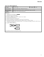
Page 56: ...EC LEVEL knob Adjust until the value of the output signals from pin 4 TE and pin 3 MPP of CN102 are the same or the differential output of these signals is minimal Procedure 1 Press the AUTO MANUAL button so that 03 F6 appears on the FL display 2 Adjust with the DIGITAL REC LEVEL knob until the above adjustment value to be reached is obtained 3 Press the DIGITAL REC LEVEL knob to register the adju...

Page 57: ...tment value to be reached is obtained Press the DIGITAL REC LEVEL knob to register the adjustment Once the adjustment is registered with the DIGITAL REC LEVEL knob on the FL display will disappear 8 Press the STOP button to stop the unit Note Adjustment must be done around mid radius on a disc 6 5 4 Focus Bias Adjustment CN102 pin 1 RF Test Point Adjustment Point Adjustment Value DIGITAL SYNCHRO b...

Page 58: ...e fuses it A thermal fuse of the power transformer fuses it IC701 Mode Controller breaks IC22 IC23 and IC25 IC protector break Check the connection of PCBs Between POWER SUPPLY assy and OPERATING assy Between POWER SUPPLY assy and CD R CORE assy FL display is dark or flickered check is displayed in the FL display Press the STOP button for 10 seconds Refer to section 7 3 1 ERROR CODE D54 Zener diod...

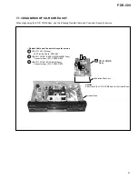
Page 59: ...t CN102 Bonnet PCB Location and Adjustment Points 2 1 2 1 2 1 2 7 1 2 DISASSEMBLY VR161 VR141 VR162 VR163 VR101 VR Assy G CD R CORE Assy OPERATING Assy I REG Assy K POWER SUPPLY Assy J DIGITAL I O Assy H HEADPHONE Assy H AUDIO Assy E ...

Page 60: ...r Binder Cut Unhook POWER SUPPLY Assy Pull up Tray Drive Gear Front Side Bridge Servo Mechanism Block Stopper CD R CORE ASSY CD R CORE Assy Servo Mechanism Block 5 CN502 CN301 CN452 CN101 CN451 CN453 CN901 1 3 2 2 3 4 6 6 1 1 3 2 4 2 5 9 8 9 9 10 7 2 3 5 2 4 2 CD R CORE Assy A ...

Page 61: ...53 CN452 1 1 3 2 CD R CORE Assy A When diagnosing the CD R CORE Assy use the following Flexible Cable and Connector Assys for service CN101 CN1 Pickup 32P Flexible Cable PDD1202 Flexible Cable and Connector Assys for service 2 CN452 CN601 SERVO MECHANISM Assy Connector Assy 9P PG09KK E35 3 CN453 CN551 LOADING B Assy Connector Assy 2P PG02KK E35 ...

Page 62: ...c c a L e t u m e g a t s t s a l O I D U A P O T S g n i r u d d n a h c t i w s r o t c e l e s t u p n i t a E S U A P C E R g n i r u d N O E T U M 5 1 3 0 P 2 0 3 P T O s t u p t u o L 6 1 4 0 P 3 0 3 P T O s t u p t u o L 7 1 5 0 P C S X E X O L 5 8 5 9 8 C L f o t u p t u o e l b a n e c n y s l a n r e t x E 8 1 6 0 P C N Y S A X O L c n y s e m a r f P I T A 9 1 7 0 P E C N E X I O d e s ...

Page 63: ... M E T A I r o s n e s e r u t a r e p m e t f o t u p n i D A 0 6 4 I N A 4 7 P C P O F R A I 1 t h g i l n r u t e r C P O g n i n n u R 1 6 5 I N A 5 7 P 2 C D W V A I 2 t h g i l n r u t e r C P O g n i n n u R 2 6 6 I N A 6 7 P Y A R T A I P M A L C N E P O n o i t i s o p g n i d a o l f o t u p n i D A 3 6 7 I N A 7 7 P 7 D A A I d e s u t o N 4 6 D D V A d d v A V 5 5 6 1 F E R V A 1 f e r...

Page 64: ...i 4 H C 4 3 1 M V O t u p t u o d e t r e v n i n o n 1 H C 4 1 5 M V O t u p t u o d e t r e v n i n o n 5 H C 5 3 1 M V O t u p t u o d e t r e v n i 1 H C 5 1 5 M V O t u p t u o d e t r e v n i 5 H C 6 3 1 T U O O t u p t u o r e i f i l p m a 1 E 6 1 5 T U O O t u p t u o r e i f i l p m a 5 E 7 3 1 N I I t u p n i d e t r e v n i r e i f i l p m a 1 E 7 1 5 N I I t u p n i d e t r e v n i r ...

Page 65: ... o l c t i B 5 1 T U O D O t u p t u o a t a d o i d u A 6 1 K L C S Y S I s f 2 1 5 r o s f 4 8 3 s f 6 5 2 t u p n i k c o l c m e t s y S 7 1 D N G D D N G l a t i g i D 8 1 D D V y l p p u s r e w o p l a t i g i D 9 1 R N N I C h c R r o t i c a p a c r e t l i f g n i s a i l a i t n A 0 2 R P N I C h c R r o t i c a p a c r e t l i f g n i s a i l a i t n A 1 2 L N N I C h c L r o t i c a p...

Page 66: ... U F X O L e s u g n i r u D 5 8 5 9 8 C L d n a r e l l o r t n o c e d o m e h t n e e w t e b n o i t a c i n u m m o c l a i r e s e h t e s u g n i r u D 2 2 6 1 P L _ T N E C O p u s t h g i l L t u p t u o p u s t h g i l D E L R E T N E C 3 2 5 1 P O C V X O n o i t a l l i c s o L L P L r e t r e v n o c S F t u o h t i w n o i t c e l e s l a t i g i d t A F F O N O L L P 4 2 4 1 P R H T...

Page 67: ...t a m y e K 5 5 5 2 1 P 2 N A C S O 2 t u p t u o x i r t a m y e K 6 5 4 2 1 P 1 N A C S O 1 t u p t u o x i r t a m y e K 7 5 3 2 1 P 0 N A C S O 0 t u p t u o x i r t a m y e K 8 5 2 2 1 P 3 N I Y E K I 3 t u p n i x i r t a m y e K 9 5 1 2 1 P 2 N I Y E K I 2 t u p n i x i r t a m y e K 0 6 0 2 1 P 1 N I Y E K I 1 t u p n i x i r t a m y e K 1 6 7 1 1 P 0 N I Y E K I 0 t u p n i x i r t a m y ...

Page 68: ...68 PDR 509 FL TUBE 7 2 2 DISPLAY PEL1099 FUNCTION ASSY V701 Anode Grid Assignment 1 35 ...

Page 69: ...69 PDR 509 Pin Assignment ...

Page 70: ... IC301 PE5109A IC351 PDJ014A H1 CHECK display Defective mechanism controller terminals Short circuiting of parts Improper power supply IC371 HD74HC573FP H2 Pre recording process does not complete and the tray does not open CHECK display Improper input voltage at the mechanism control terminals pins 22 23 24 IC201 PA9007A H5 Pre recording process disabled CHECK display Improper IC303 data writing D...

Page 71: ...efective laser diode Defective focus drive circuits Defective pickup Improper soldering Pattern short Trouble of power supply IC451 M56788FP IC401 CXD2585Q A The unit stops in a recording related operation displaying CHECK DISC Unable to focus Stop during recording The unit stops being obstructed by a dirt or a crack on the disc If any hardware trouble occurs before displaying A or d the unit stop...

Page 72: ...monitor record record pause modes q ANALOG REC LEVEL Sets the recording level for analog input recording Outside ring controls left input level inside dial controls right input level w TRACK NUMBER AUTO MANUAL Switches between automatic and manual track number ing when recording a disc Indicator lights to remind you when manual track numbering has been turned on e TRACK NUMBER WRITE MANUAL Press d...

Page 73: ...73 PDR 509 MONITOR DIGITAL REC LEVEL ANALOG REC LEVEL INPUT SELECTOR TIME REPEAT ...

Page 74: ...ause mode r TRACK NUMBER AUTO MANUAL Switches between automatic and manual track number ing when recording a disc Front panel indicator lights to remind you when manual track numbering has been turned on t TRACK NUMBER WRITE MANUAL Press during recording to start a new track number when in manual track numbering mode y 3 Press to play or resume playing a disc Also use to start recording from recor...

Page 75: ... is in automatic synchro recording mode q D VOL Lights when the digital volume control function is active w AUTO TRACK Lights when automatic track numbering is on during recording e REC Lights to indicate recording or record pause mode Blinking display indicates record muting r Recording level meter Displays the input level during recording or the re corded level during playback t OVER indicator I...

Page 76: ...ject lens out 3 beam total 23 mW Laser class ΙΙΙb 8 2 SPECIFICATIONS KU CA Type MY and MV Types 1 General Model Compact disc audio system Applicable discs CDs CD Rs and CD RWs Power supply AC 220 230 V 50 60 Hz Power consumption 18 W Operating temperature 5 C to 35 C Weight without package 3 9 kg Max dimensions 420 W 300 D 105 H mm 2 Audio unit Frequency characteristics 2 Hz to 20 kHz Playback S N...

Page 77: ...IP ID CLEAR AUTO MANUAL TRACK NO WRITE REC 1 2 3 4 5 6 7 8 9 10 0 10 COMPACT DISC RECORDER REMOTE CONTROL UNIT Two Sets of Audio Cords PDE1249 L 1 m AC Power Cord KU CA Type ADG7021 Two AA size R6P Batteries VEM 013 Remote Control Unit CU PD114 PWW1163 AC Power Cord MV Type ADG7004 AC Power Cord MY Type ADG1127 White Red White Red ...

Reviews: