background image

PRV-LX10

132

1

2

3

4

1

2

3

4

C

D

F

A

B

E

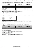
In the service_info.log file, detailed data on Service Info, which can be accessed by 
selecting Function Menu, System, Information, then Service Info, are recorded, as shown 
below:

<<<<< Start PRV-LX10 >>>>>   Mon Oct 20 06:25:22 EDT 2003
  -- HDD SMART:Val(Max)/Thrsh --<<Spare Sector>> fd(fd)/3f  <<Sk ErrRate>> fd(fc)/00
<<Spdl Mtr Retry>> fd(fc)/9d <<W ErrRate>> fd(fc)/00 Lecel=0
  !!!!!<<<<< PCI Access Error Count = 1  >>>>> (Date) Mon Oct 20 06:25:51 EDT 2003
  !!!!!<<<<< PCI Access Error Count = 2  >>>>> (Date) Mon Oct 20 06:27:23 EDT 2003
  <<Check HDD SMART Data>>:Mon Oct 20 06:28:15 EDT 2003
  -- HDD SMART:Val(Max)/Thrsh --<<Spare Sector>> fd(fd)/3f  <<Sk ErrRate>> fd(fc)/00
<<Spdl Mtr Retry>> fd(fc)/9d <<W ErrRate>> fd(fc)/00 Lecel=0
<<<<< Start PRV-LX10 >>>>>   Mon Oct 20 06:30:43 EDT 2003
  -- HDD SMART:Val(Max)/Thrsh --<<Spare Sector>> fd(fd)/3f  <<Sk ErrRate>> fd(fc)/00
<<Spdl Mtr Retry>> fd(fc)/9d <<W ErrRate>> fd(fc)/00 Lecel=0
<<<<< Start PRV-LX10 >>>>>   Mon Oct 20 07:09:38 EDT 2003
  -- HDD SMART:Val(Max)/Thrsh --<<Spare Sector>> fd(fd)/3f  <<Sk ErrRate>> fd(fc)/00
<<Spdl Mtr Retry>> fd(fc)/9d <<W ErrRate>> fd(fc)/00 Lecel=0

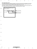
1

Time when the PRV-LX10 starts up

2

Data from "--HDD SMART:Val(max)/Thrsh--" to "Level=0" indicate SMART data regarding the built-in HDD confirmed when
the PRV-LX10 starts up. The results of confirmation on SMART data are recorded in the log file when System is selected by
opening Function Menu then System, as well as at startup. The levels of self-diagnosis results are as shown below. 
It should be noted that the descriptions of the levels are different from those used on the Function Menu. 
For details, see "Levels of the self-diagnosis results of the HDD and measures to be taken for them."
0: Normal operation
1: Level calling for the user's attention (indicated as 0+ on the Function Menu)
2: Level calling for the user's attention (indicated as 1 on the Function Menu)
3: Warning symptoms of an HDD failure (indicated as 2 on the Function Menu)
4: On the brink of an HDD failure (indicated as 3 on the Function Menu)
5: HDD failure (indicated as 4 on the Function Menu)

3

A total number of errors generated on the PCI bus after the PRV-LX10 starts up is recorded (Each time the power is turned
on, the number of errors is counted from 0). If errors are frequently generated, it may because of a defective Motherboard
or PCI board, or poor connection caused by inappropriate installation of the PCI board. Error data are recorded in the log
file each time an error is generated. Error data are also indicated on the Service Info page, which can be accessed by
selecting Function Menu, System, Information, then Service Info, only when an error is generated (the first figure indicates
the level of the self-diagnosis results of the HDD, and the second indicates the total number of PCI bus errors).

4

Each time the unit starts up, and each time System is selected (select Function Menu then System), the level of the self
-diagnosis results of the HDD is confirmed and recorded in the log file. Data from "<<Check HDD SMART Data>>" to
"Level=0" are the results of confirmed SMART data to be recorded when System is selected (select Function Menu then
System).

Details on the log file (service_info.log)

1

1

3

3
4

4

2

2
1

2

Summary of Contents for PRV-LX10

Page 1: ...NTRE PTE LTD 253 Alexandra Road 04 01 Singapore 159936 PIONEER CORPORATION 2005 PRV LX10 RRV3069 DVD RECORDER PRV LX10 THIS MANUAL IS APPLICABLE TO THE FOLLOWING MODEL S AND TYPE S Before returning the repaired product to the user be sure to upgrade the firmware to its latest version Model Type Power Requirement Remarks PRV LX10 WYV RB AC220 240V For details refer to Important Check Points for goo...

Page 2: ...re often not evident from visual inspection nor the protection afforded by them necessarily can be obtained by using replacement components rated for voltage wattage etc Replacement parts which have these special safety characteristics are identified in this Service Manual Electrical components having such features are identified by marking with a on the schematics and on the parts list in this Se...

Page 3: ...G OPERATION OF THE APPARATUS SHOULD BE DONE BY A SPECIALLY INSTRUCTED PERSON LASER DIODE CHARACTERISTICS MAXIMUM OUTPUT POWER 25 mW WAVELENGTH 654 662 nm LASER DIODE CHARACTERISTICS MAXIMUM OUTPUT POWER 36 mW WAVELENGTH 780 787 nm LABEL CHECK DRW2109 DRW2185 DRW2162 DRW2069 DRIVE Assy LX1 Note You will see one of the following two labels attached ...

Page 4: ...the product Please check that neither solder debris nor screws remain inside the product 8 There should be no semi broken wires scratches melting etc on the coating of the power cord Damaged power cords may lead to fire accidents so please be sure that there are no damages If you find a damaged power cord please exchange it with a suitable one 9 There should be no spark traces or similar marks on ...

Page 5: ...IAGRAM 40 3 3 JKIB ASSY 1 3 42 3 4 JKIB ASSY 2 3 44 3 5 JKIB ASSY 3 3 46 3 6 JKDB and 422IB ASSYS 48 3 7 HPVB and JKOB ASSYS 50 3 8 DECB ASSY 1 2 52 3 9 DECB ASSY 2 2 54 3 10 PCIB ASSY 1 4 56 3 11 PCIB ASSY 2 4 58 3 12 PCIB ASSY 3 4 60 3 13 PCIB ASSY 4 4 62 3 14 AVIB ASSY 1 6 64 3 15 AVIB ASSY 2 6 66 3 16 AVIB ASSY 3 6 68 3 17 AVIB ASSY 4 6 70 3 18 AVIB ASSY 5 6 72 3 19 AVIB ASSY 6 6 74 3 20 PWRB ...

Page 6: ... GENERAL INFORMATION 117 7 1 DIAGNOSIS 117 7 1 1 TESTMODE 117 7 1 2 TEST MODE CODE 120 7 1 3 LED SPECIFICATIONS 122 7 1 4 POWER ON SEQUENCE 127 7 1 5 HOW TO CHECK THE ERROR LOG 130 7 1 6 ERROR LOG DISPLAY 135 7 1 7 DEBUGGING DISPLAY MODE 139 7 1 8 LIST OF BIOS SETTING VALUE 143 7 1 9 REWRITING OF THE GUIDS 145 7 1 10 CAUTIONS ON HANDLING THE HDD 146 7 1 11 HDD REPLACEMENT PROCEDURES 148 7 1 12 HOW...

Page 7: ...ity 85 or less Note Because the HDD is mounted on the unit be sure not to impart shock or vibration to the unit while it is operating For the test of the unit use the following recommended media DVD R GGV1139 DVD RW GGV1050 Test Specifications Conditions and connections for the test Conditions for the test Standard Phones Impedance 32Ω Keyboard to be connected to the USB connector TK U109JPW2 manu...

Page 8: ... be recognized on startup B B ROUTER Manufactured by I O data NP BBRE or equivalent AV AMP Manufactured by Pioneer VSA C100 or equivalent Video SG NTSC MG6301A or equivalent PAL TG19CA or equivalent Black Burst Media Converter Manufactured by data video DAC 100 or equivalent Audio Analyzer RCA AD725C or equivalent XLR AM51A or equivalent DVD Player Video SG NTSC S CV MG6301A or equivalent Componen...

Page 9: ...of Titles 0 Last Modified Date yyyy mm dd hh mm ss Total Capacity 0 MB Copy Project Copy To Copy Clip Copy From No Item Source Drive HDD Clip No Item Delete Delete No Item DVD Disc Make Disc Image Target Image hyymmdd_xx img Target DVD 1 APP Auto Capture IN OUT Point Preroll Time 5 Seconds Offsest Frame 17 Frames Record As Title Stop IN OUT Point 00 00 00 00 Chapter Point Chapter Point 00 00 00 00...

Page 10: ...Network OFF DHCP Manual DHCP MAC Address UPS Setting Model Disabled Shutdown Delay 30 seconds x xx x x xx Information System Version Power On Time xxxx h HDD Access xxxx h Drive 1 R W xxxx h xxxx h Service Info x Remaining Capacity 100 87 GB Drive 2 R W xxxx h xxxx h HDD Tools Target Drive HDD Operation Control Settings Control Local Port RS 422A Time Code RS 422A Eject Setting Eject Video Setting...

Page 11: ...ding Video Audio Video Encode Rate 9 644Mbps Video Filter NR OFF Audio Encode Dolby Digital Audio Level L 0 R 0 Aspect 4 3 Setup Level Blank Others Auto Chapter Manual REC Button REC Start Playback Video Aspect 4 3 LB Still Mode Frame Audio Dolby Digital OUT Dolby Digital DTS OUT OFF 96kHz PCM OUT Convert To 48kHz MPEG OUT MPEG Language Audio English Subtitle English DVD Menu English Others Parent...

Page 12: ...Sampling frequency 48 kHz Compression format Dolby Digital and Linear PCM non compressed Recording time DVD R RW manual rate About 1 6 hours HDD manual rate About 23 100 hours Playback Playable discs DVD Video DVD R DVD RW CD R CD RW and CD ROM are supported for data read only Video input Composite BNC x 1 1 0 Vp p 75 Ω S VIDEO 4 pin mini DIN x 1 Y 1 0 Vp p 75 Ω C 0 286 Vp p NTSC 0 300 Vp p PAL 75...

Page 13: ... male x 2 0 dBu 600 Ω load low impedance Frequency response 4 Hz to 22 kHz DVD fs 48 kHz S N ratio More than 60 dB Distortion THD N Less than 0 02 Digital unbalanced Pin jack x 1 0 5 Vp p 75 Ω External Sync Input BNC x 2 black burst 0 286 Vp p NTSC 0 300 Vp p PAL 75 Ω ON OFF Other DV input output 4 pin i Link IEEE 1394 compatible x 1 LTC input BNC x 1 0 5 8 Vp p 3 kΩ Remote input D sub 9 pin femal...

Page 14: ...s indicates the importance of the safety factor of the part Therefore when replacing be sure to use parts of identical designation Screws adjacent to mark on product are used for disassembly For the applying amount of lubricants or glue follow the instructions in this manual In the case of no amount instructions apply as you think it appropriate NOTES 23 19 13 14 15 16 6 5 10 21 22 10 22 20 17 18 ...

Page 15: ...P 7 Dry Cell Battery R6P AA VEM1031 NSP 8 Polyethylene Bag Z21 004 60 x 120 x 0 03 NSP 9 Polyethylene Bag Z21 010 100 x 230 x 0 018 NSP 10 Polyethylene Bag Z21 019 235 x 320 x 0 06 11 Bottom Pad DHA1571 12 13 Accessory Plate DHA1651 14 Accessory Plate 2 DHA1652 15 Accessory Base DHA1653 16 Top Pad 2 DHA1655 17 F Pad 2 DHA1656 18 R Pad 2 DHA1657 19 FE Sheet 2 DHA1675 20 Packing Case EU DHG2456 21 M...

Page 16: ...N Refer to 2 6 FRONT PANEL SECTION 5 6 4 6 1 1 2 3 3 3 3 3 3 3 2 5 7 3 2 3 8 10 10 14 13 12 13 14 14 11 9 18 18 18 18 18 18 18 18 18 18 17 17 17 17 17 17 17 17 17 17 17 19 19 19 17 17 Gasket B Bonnet 16 10 12 15 1 17 Note 1 When removing the front panel section be sure to remove this screw Note 2 Gasket locations 11 12 To PWRB CN3 To MOTHER COM2 ...

Page 17: ...rk No Description Part No Note 3 Notes on locations where gaskets are adhered At the locations where gaskets are to be adhered on each part engraved marks are provided a Rectangular gaskets Adhere a rectangular gasket by aligning it with the engraved corner marks If no marks are provided on the part adhere the gasket aligned with the four corners of the part b L shaped gaskets Adhere an L shaped g...

Page 18: ...te 1 When disassembling reassembling No 6 Drive Assy LX1 make sure that No 11 Silicone spacer A is not torn or damaged If it is replace with a new one Note 4 Attach the earth spring AVIB CU after the AVI base EU AVI shield EU and AVIB Assy have been assembled but before they are reassembled into the unit Note 2 When replacing JKIB Assy or JKOB Assy be sure to remove 3P BNC earth plate BNC earth pl...

Page 19: ...EC1850 31 DC Fan Motor AXM7014 NSP 32 Fan Duct EU DNK4447 33 Gasket RB DEC2742 34 Gasket FC DEC2802 35 Screw BBZ30P060FMC 36 Screw AMZ30P060FZK 37 Screw BPZ30P350FZK 38 Screw BPZ30P080FZK 39 Screw BBT30P060FZK 40 Screw PPZ30P100FMC 41 EMC Sheet S DEB1624 42 EMC Sheet DEB1620 43 Binder DEC2803 44 Gasket AVI DEC2747 45 3P BNC Earth Plate CU DBK1273 46 BNC Earth Plate CU DBK1274 47 Earth Spring AVIB ...

Page 20: ... 46 46 46 46 50 50 50 50 50 46 48 48 10 33 46 46 45 58 26 36 36 36 17 41 43 44 44 51 51 42 56 56 42 40 3 15 26 30 54 31 15 16 17 46 46 47 12 13 47 14 Refer to 2 5 REAR PANEL SECTION 53 53 32 53 53 53 57 57 57 57 46 52 To USSB CN684 To AVIB CN3201 To FLKB CN501 To Fan Left To Drive Assy To Fan Right 1 2 Note 1 Be careful of sharp edges while working around this section Note 2 When the HDD is remove...

Page 21: ...642 26 Binder ZCA SKB90BK NSP 27 Main Chassis EU DNA1312 NSP 28 PCB Support VEC1267 29 Card Spacer QEC1012 30 Label for service BAX1238 NSP 31 Label VRW 348 32 Lithium Battery Caution Label DRW2162 33 Connector Assy 6P DKP3644 34 Edge Guard A DEC2566 NSP 35 Wire Saddle DEC2543 NSP 36 Wire Saddle 8S DEC1760 37 Connector Assy 20P DKP3657 38 Connector Assy 2P DKP3736 39 Connector Assy 14P DKP3636 40 ...

Page 22: ...08 To PWRB CN9 B C 1 2 14 7 14 20 4 17 Gasket RP 18 6 9 10 11 13 Torque 0 65 N m 5 15 19 16 12 Note When removing the JKDB Assy or 4221B Assy be sure to remove the rear panel first Note When replacing the JKDB Assy be sure to remove the 3P BNC earth plate CU from the old Assy and attach it to the new Assy Note Gasket locations ...

Page 23: ...SP 5 Terminal Cover DNK4154 NSP 6 Blind Plate DNF1678 7 Earth Terminal DKE 102 NSP 8 Guard Tape DEC2587 9 Fan Spacer AMR7265 10 DC Fan Motor AXM7014 11 Fan Cover AMR7264 12 Fan Plate DEC2692 13 Screw ABA7003 14 Screw BBT30P060FZK 15 Screw BBA1051 16 3P BNC Earth Plate CU DBK1273 17 Gasket RP DEC2743 18 Rear Panel Assy DXA2022 19 Washer WH30FNI 20 Screw BBZ30P060FMC ...

Page 24: ... 32 36 36 36 36 36 36 31 36 34 36 35 16 14 15 39 38 15 1 1 2 Note 1 This part must be placed with the correct side facing up Be careful of the direction during attachment Note 2 for lead dressing Do NOT bend the flexible cable at points very near the reinforcing plates that are provided at the two ends of the flexible cable Such bending may lead to breakage of the cable Note For this screw use a m...

Page 25: ...1043 19 Power Button DAC2105 20 IR Window DNV1042 21 Drive Lens DNV1039 22 Tray Button 1 DAC2099 23 Flexible Cable 6P DDD1231 24 ETC Button DAC2103 25 Drive Select Lens DNV1041 26 Cursor Button DAC2104 27 Drive Select Button DAC2102 28 Preview Button DAC2107 29 Play Button 1 DAC2100 30 Play Button 2 DAC2101 31 Earth Metal B CU DBK1277 32 Barrier FL DEC2748 33 Barrier 2 DEC2533 34 Flexible Cable 25...

Page 26: ...IDEO ENCODER DVxcel 168 180 IC4002 TSB41AB2PAP DV Phy IC4001 TSB42AB4PDT DV Link 1 13 2 3 4 5 CN4001 6P 34 XTPB TPB XTPA TPA 35 36 37 19 82 96 77 20 23 1 9 19 24 2 12 CN3002 50P 11 26 CN6002 30P 6 8 2 29 AV1 AUDIO DATA 81 89 68 70 DV OUT 656 ANALOG 28 30 1 3 5 7 7P CN3202 9V 9V 9V 5V CN3001 50P MPU BUS X3301 27MHz VCXO PCO IC5002 PD6342A TBC DNR Vaikilt 44 54 117 126 55 64 156 165 131 PCO 29 27 27...

Page 27: ..._O PWR_SW 5V V 24V V 28V V 31V V 28V V 24V IC501 uPD78F0058GC FL uCOM 3 4 7 CN501 20P 8 10 12 13 6 9 14 16 18 15 17 19 3 2 3 2 CN504 3P 9 8 IC503 PT6315 FL DRV IC502 PT6315 FL DRV V502 DAW1019 FL TUBE V501 DAW1019 FL TUBE 11 14 15 18 6 9 6 9 V 31V V 5V S501 S507 KEY UP RIGHT DOWN LEFT ENTER SETUP DISPLAY CN503 25P 6 12 24 13 16 20 23 V 5V 6 40 53 54 37 39 43 52 5 38 50 51 V 5V CN601 25P 2 10 13 14...

Page 28: ...Cr JA7854 AMP SMPTE AMP Beta AMP SMPTE COMP CN7611 CN7402 CN7801 CN7851 CN661 CN7941 CN7902 CN7903 CN7952 CN7802 CN7701 CN7613 AMP AMP AMP AMP Thru Thru Y Cb Cr LTR SQZ L R JA7851 JA7981 JA661 Y C CV JA7855 SPDIF XLR CH1 L XLR CH2 R 6dB Y C IC7803 CV SPDIF L R MUTE MUTE 6dB P I Y Cb Cr Y C CV 5V V Select 2 Thru A Select Beta SMPTE 9V 9V 9V Thru XLR CH2 R Thru SYNC SEP 422 DRV RCV Ex Sync LTC JA794...

Page 29: ...DRAM IC1851 IC1853 ANALOG SW IC1711 VIDEO Enc IC1751 AUDIO DAC IC1513 MPEG Dec AV 1 IC1211 MPU SH 3 PCI BUS SH 3_ADRS SH 3_DATA SH 3_CTRL MPEG_ BITSTREAM Y Pb Pr Y Cb Cr Component Composite S VIDEO Y C Audio L R Digital AV Signal Analog Video Signal Analog Audio Signal Digital Signal and Control Signal AV 1_VIDEO AV 1_AUDIO P XI ...

Page 30: ... Xilinx IC2001 PD5219 Slalom DMA Control CPU IF etc IC2003 HY57V641620HGT 7 64M SDRAM Stream Buffer IC2404 K4S643232H TC60 64M SDRAM Main Memory MOTHER BOARD ASSY PCIB ASSY CN2405 7 pin CN1183 7 pin CN2101 4 pin CN2103 50 pin CN2104 50 pin CN3301 4 pin CN3002 50 pin CN3001 50 pin CN2102 11 pin CN7902 11 pin CN2301 CN2302 PCI Card Edge 124 pin JKDB ASSY B DECB ASSY F AVIB ASSY H G ...

Page 31: ..._A1 9 L_A1 9 L_A0 15 C_A0 15 L_D0 15 C_D0 15 L_D0 15 L_A1 3 IC5004 LTC_SW XILINX IC5002 Vaikilt TBC DNR IC5001 64M SDRAM IC7004 DVXcel MPEGENC DV CODEC IC7002 64M SDRAM IC7003 64M SDRAM IC3002 IC3003 BUF IC3002 IC3003 BUF IC3004 BUF IC4001 DV Link IC4002 DV Physical VCXO 27MHz Oscillation Block From Vaikilt IC3309 PLL1700 PLL IC IC3310 BUF IC3308 27MHz BUF To SDIB From SDIB 27MHz which was locked ...

Page 32: ...KAU LRCKAU ADATSO BCKSOI LRCKSO ADATSI BCKSI LRCKSI ADATX BCKAPX LRCKX ADATDV BCKDV LRCKDV IC7002 64M SDRAM IC7003 64M SDRAM CN4001 CN3001 DV Stream data DV Stream data 1394 Differential DVI0 7 PHY0 7 L_D0 7 L_D0 15 L_D0 15 L_A0 7 L_A1 9 L_A0 15 L_A0 15 C_A0 15 L_D0 15 C_D0 15 L_D0 15 L_A1 3 IC3002 IC3003 BUF IC3004 BUF IC4001 DV Link IC4002 DV Physical Host Address Data Bus Host Address Data Bus ...

Page 33: ... CN684 CN681 CN2 Serial Communication Block LED Block AVIB Block SW Block SIN SOUT V 5V_FLK USB 5V D1 D1 D2 D2 FANCONT Rear PWR_OK PWR_SW PS_ON 5VSB ATX PSU MOTHER BOARD ASSY 3 3 5 12V 5VSB PWR_OK 3 3 5 12V PWR_OK 5V FANCONT DRV1 FANCONT DRV2 FLKB ASSY KEYB ASSY DRV2B ASSY DRV1B ASSY USBB ASSY PWRB ASSY LED Block LED Block LED Block SW Block SW Block SW Block CN602 CN641 CN4 CN1 CN504 COM2 9 3 2 1...

Page 34: ... FAN_CONT Rear FLKB ASSY FLKB ASSY AVIB ASSY AVIB ASSY FAN PWR_SW Power Control Block 5VSB 5VB FAN FAN FAN Detection Block FAN Power Control Block 3 3V 5V 12V 12V 5V 2 5V Power Generation Block 3 3V Power Generation Block 12V Power Generation Block 24V FL Power Generation Block 23 5V 28V FL Power Generation Block 27 0V 31V FL Power Generation Block 30 5V PWRB POLY ASSY I To ATX POWER SUPPLY UNIT ...

Page 35: ...16 IC7803 pin 33 CVBS OUT V 1V div H 10µsec div 22 IC7803 pin 31 S C OUT V 1V div H 10µsec div 5 IC7420 pin 7 Cr Beta IN V 1V div H 10µsec div 11 IC7613 pin 1 RCA_L IN V 2V div H 1msec div 17 IC7803 pin 28 S Y OUT V 1V div H 10µsec div 23 IC7803 pin 25 Prog Y G OUT V 1V div H 10µsec div 6 IC7404 pin 7 CV_THRU IN V 1V div H 10µsec div 12 IC7613 pin 7 L_THRU IN V 2V div H 1msec div 18 IC7803 pin 25 ...

Page 36: ...in 33 CV_THRU OUT V 1V div H 10µsec div GND 46 IC7803 pin 31 S_C OUT V 1V div H 10µsec div GND GND 39 IC7402 pin 5 SYNC PULS V 1V div H 10µsec div GND 41 IC7803 pin 28 S_Y OUT V 1V div H 10µsec div GND 42 IC7803 pin 25 Y G OUT V 1V div H 10µsec div GND GND GND GND GND GND GND A 3 3 A 2 3 A 2 3 A 2 3 A 2 3 A 3 3 31 IC7409 pin 7 CVBS IN V 1V div H 10µsec div 32 IC7409 pin 7 S_Y IN V 1V div H 10µsec ...

Page 37: ...S Y V 0 5V div H 10µsec div 8 CN1811 pin 16 Y prog V 0 5V div H 10µsec div 3 CN1811 pin 16 Y V 0 5V div H 10µsec div 9 CN1811 pin 18 Cb prog V 0 5V div H 10µsec div 4 CN1811 pin 18 Cb V 0 5V div H 10µsec div 10 CN1811 pin 20 Cr prog V 0 5V div H 10µsec div 5 CN1811 pin 20 Cr V 0 5V div H 10µsec div 6 CN1611 pin 23 Lch V 2V div H 1msec div DECB ASSY F GND GND GND GND GND GND GND GND GND GND F 2 2 F...

Page 38: ...n 13 Cr Beta SMPTE V 1V div H 10µsec div DECB ASSY F AVIB ASSY H AVIB ASSY H GND GND GND GND GND GND GND GND GND GND GND GND GND F 2 2 F 2 2 F 2 2 H 2 6 H 2 6 H 2 6 H 2 6 H 2 6 H 2 6 H 2 6 F 2 2 F 2 2 F 2 2 8 CN3501 pin 7 CVBS V 1V div H 10µsec div 9 CN3501 pin 7 S Y V 1V div H 10µsec div 10 CN3501 pin 9 S C V 1V div H 10µsec div 11 CN3501 pin 7 Y V 1V div H 10µsec div 12 CN3501 pin 11 Cb V 1V div...

Page 39: ...PRV LX10 39 5 6 7 8 5 6 7 8 C D F A B E ...

Page 40: ...Y DWZ1133 C HPVB ASSY DWZ1128 D F 1 2 F 2 2 DECB ASSY DWP1081 F G 1 4 G 4 4 PCIB ASSY DWP1080 G H 1 6 H 6 6 AVIB ASSY DWV1202 H 27MHz CLOCK ADJ AKM1278 AKM1293 AKM1275 DKP3673 DKP3674 DDD1266 AKM1292 AKN7032 AKM1277 DDD1267 DDD1267 AKM1275 AKM1300 JKOB ASSY DWZ1127 E A 1 3 A 3 3 JKIB ASSY DWZ1126 A ...

Page 41: ... 120G 4R120L0 VXF1015 DRIVE ASSY LX1 DXX2532 DRIVE ASSY LX1 DXX2532 ATX POWER SUPPLY UNIT DXF1005 Rear Left Right DC FAN MOTOR FRONT AXM7014 DC FAN MOTOR REAR AXM7014 DKP3676 VKN1943 AKM1274 AKM1274 DKP3671 DKP3671 AC 220 240V 50 60Hz AC POWER CORD ADG1214 FLKB WYV RB ASSY DWZ1164 J Note When ordering service parts be sure to refer to EXPLODED VIEWS and PARTS LIST or PCB PARTS LIST ...

Page 42: ...ector Input Video Thrugh Selector 4 1VDC 4 3VDC 1 8VDC 2 5VDC 2 4VDC 1 9VDC 2 5VDC 1 7VDC 1 8VDC 2 5VDC 2 5VDC 1 8VDC 2 5VDC 3 5VDC 3 5VDC 2 5VDC 3 4VDC 3 4VDC 2 5VDC 2 5VDC 2 5VDC 4 3VDC 4 3VDC 1 8VDC 5 0VDC 5 0VDC 6dB 6dB 6dB 5 8dB 2 8dB 2 8dB A 1 3 JKIB ASSY DWZ1126 VKN1072 R_A R_V R_V R_V R_V R_GY R_GY R_GY R_GY R_Y R_GY R_GY R_Y R_Y R_Y R_C R_C R_C R_C R_Cb R_Cb R_Cb R_Cb R_Cb R_Cr R_Cr R_Cr ...

Page 43: ...VDC 6 5VDC 6 0VDC 6 0VDC 4 9VDC 4 2VDC 4 9VDC 4 2VDC 4 5VDC 7dB AKM1277 Recording Signal Route Composite Video R_V Recording Signal Route S Video_Y R_Y Recording Signal Route Component_Y R_GY Recording Signal Route S Video_C R_C Recording Signal Route Component_Cb R_Cb Recording Signal Route Component_Cr R_Cr Recording Signal Route Analog Audio L ch R_A Recording Signal Route Digital Audio Video R...

Page 44: ... Input Audio Through Selector Input Audio Through Selector Input Audio Through Selector Relay for Audio Mute 0dB 0dB 0dB 0dB 0dB 0dB 0dB 0dB 9dB 9dB 0VDC 0VDC 0VDC 0VDC 0VDC 0VDC 2 8V 0 1V A 2 3 JKIB ASSY DWZ1126 CEVWNP100M25 CEVWNP100M25 CEVWNP100M25 CEVWNP100M25 BTH1119 BTH1119 AKM1278 BTH1119 BTH1119 R_A R_A R_A R_A R_A R_A R_A R_A R_A R_A R_V R_GY R_Y R_C R_Cb R_Cr 12 13 11 ...

Page 45: ...wn with the marked box CEVWNP470M10 CEVWNP470M10 CEVWNP470M10 CEVWNP470M10 CEVWNP470M10 CEVWNP470M10 Recording Signal Route Composite Video R_V Recording Signal Route S Video_Y R_Y Recording Signal Route S Video_C R_C Recording Signal Route Component_Cb R_Cb Recording Signal Route Component_Cr R_Cr Recording Signal Route Analog Audio L ch R_A Playback Signal Route Analog Audio L ch P_A P_A P_A P_A...

Page 46: ...yback Signal Route Composite Video P_V Playback Signal Route S Video_Y P_Y Playback Signal Route S Video_C P_C Playback Signal Route Component_Cb P_Cb Playback Signal Route Component_Cr P_Cr Recording Signal Route Analog Audio L ch R_A Playback Signal Route Analog Audio L ch P_A R_A R_A P_A P_A P_V P_Y P_GY P_C P_Cb P_Cr Playback Signal Route Digital Audio P_D P_D P_D P_D P_D P_V P_GY P_Y P_C P_Cb...

Page 47: ...PRV LX10 47 5 6 7 8 5 6 7 8 C D F A B E ...

Page 48: ...PRV LX10 48 1 2 3 4 1 2 3 4 C D F A B E 3 6 JKDB and 422IB ASSYS B C CN1471 F 2 2 JKDB ASSY DWZ1134 B 422IB ASSY DWZ1133 C LTC Comparator 0V 0V 0V 0V 1 2 4 ...

Page 49: ...PRV LX10 49 5 6 7 8 5 6 7 8 C D F A B E IB B CN2102 G 2 4 RS 422 Driver Receiver The power supply is shown with the marked box ...

Page 50: ...wn with the marked box Playback Signal Route Composite Video P_V Playback Signal Route S Video_Y P_Y Playback Signal Route S Video_C P_C Playback Signal Route Component_Cb P_Cb Playback Signal Route Component_Cr P_Cr Playback Signal Route Analog Audio L ch P_A Playback Signal Route Digital Audio P_D P_A P_A P_A P_A 1 Playback Signal Route Component_Y P_GY ...

Page 51: ... 5 6 7 8 5 6 7 8 C D F A B E E CN7802 A 3 3 JKOB ASSY DWZ1127 E P_A P_A P_A P_A P_A P_A P_A P_A P_A P_A P_A P_A P_D P_D P_D P_D P_V P_V P_V P_V P_GY P_GY P_Y P_Y P_Y P_C P_C P_C P_Cb P_Cb P_Cr P_Cr P_GY P_Cb P_Cr ...

Page 52: ...PRV LX10 52 1 2 3 4 1 2 3 4 C D F A B E 3 8 DECB ASSY 1 2 F 1 2 F 1 2 DECB ASSY DWP1081 3 3V Reg 2 5V Reg 1 8V Reg MPU IC ...

Page 53: ...own with the marked box F 1 2 MOTHER BOARD ASSY J2 PCI SLOT F 2 2 F 2 2 F 2 2 Reset IC Playback Signal Route Digital Audio Video P_DAV P_DAV CAUTION FOR CONTINUED PROTECTION AGAINST RISK OF FIRE REPLACE ONLY WITH SAME TYPE NO ICP S2 3 MFD BY ROHM CO LTD FOR IC1351 ...

Page 54: ...V Playback Signal Route S Video_Y P_Y Playback Signal Route Component_Y P_GY Playback Signal Route S Video_C P_C Playback Signal Route Component_Cb P_Cb Playback Signal Route Component_Cr P_Cr Playback Signal Route Digital Video P_DV Playback Signal Route Analog Audio L ch P_A Playback Signal Route Digital Audio P_D Playback Signal Route Digital Audio Video P_DAV P_DV P_DV P_D P_D P_D P_D P_D ...

Page 55: ...36V 0 46V 1 1V 1 1V 0 46V 0V 0 32V 0V 0 67V 0 64V 1 3V 0 64V 0 95V 0 64V 1 9V 0V 1 2V 2 5V 0 67V 0 99V 0 99V 0 99V 1 3V 2 5V Display Black V Progressive P_DV P_DV P_D P_D P_D P_D P_DV P_D P_A P_A P_A P_A P_V P_V P_V P_Y P_GY P_GY P_GY P_GY P_Y P_Y P_C P_C P_C P_Cb P_Cb P_Cb P_Cb P_Cr P_Cr P_Cr P_Cr 1 11 7 16 2 12 3 4 8 13 9 14 5 10 15 6 K4S643232H TC60 PD6454D8 ...

Page 56: ...PRV LX10 56 1 2 3 4 1 2 3 4 C D F A B E 3 10 PCIB ASSY 1 4 G 1 4 G 3 4 G 3 4 G 2 4 G 4 4 DMA Control CPU I F etc R_DAV R_DAV R_DAV R_DAV ...

Page 57: ...PRV LX10 57 5 6 7 8 5 6 7 8 C D F A B E G 1 4 G 1 4 PCIB ASSY DWP1080 G 2 4 4 4 G 2 4 3 4 Stream Buffer Recording Signal Route Digital Audio Video R_DAV R_DAV ...

Page 58: ...PRV LX10 58 1 2 3 4 1 2 3 4 C D F A B E 3 11 PCIB ASSY 2 4 G 2 4 CN7902 CN3001 H 1 6 G 3 4 G 1 4 3 4 4 4 G 1 4 3 4 B G 1 4 3 4 4 4 G 1 4 3 4 4 4 3 5 Converter ...

Page 59: ...PRV LX10 59 5 6 7 8 5 6 7 8 C D F A B E G 2 4 G 2 4 PCIB ASSY DWP1080 CN3301 H 1 6 CN3002 H 1 6 G 4 4 G 1 4 G 1 4 Recording Signal Route Digital Audio Video R_DAV R_DAV R_DAV ...

Page 60: ...PRV LX10 60 1 2 3 4 1 2 3 4 C D F A B E 3 12 PCIB ASSY 3 4 G 3 4 G 3 4 PCIB ASSY DWP1080 MOTHER BOARD ASSY J3 PCI SLOT G 4 4 G 1 4 G 1 4 G 4 4 G 4 4 G 2 4 Reset IC ...

Page 61: ...PRV LX10 61 5 6 7 8 5 6 7 8 C D F A B E The power supply is shown with the marked box G 3 4 G 4 4 G 1 4 2 4 4 4 G 1 4 2 4 G 2 4 PCI I F XC2S100 5PQ208C ...

Page 62: ...PRV LX10 62 1 2 3 4 1 2 3 4 C D F A B E 3 13 PCIB ASSY 4 4 G 4 4 G 3 4 MPU 5 3 Converter ...

Page 63: ...PRV LX10 63 5 6 7 8 5 6 7 8 C D F A B E G 4 4 G 4 4 PCIB ASSY DWP1080 G 3 4 G 3 4 G 1 4 G 1 4 3 4 G 3 4 G 3 4 G 1 4 G 1 4 Main Memory Flash ROM PD6453D8 K4S643232H TC60 ...

Page 64: ... 14 AVIB ASSY 1 6 H 1 6 H 1 6 CN2104 G 2 4 CN2103 G 2 4 AVIB ASSY DWV1202 4 6 H 2 6 6 6 H 2 6 6 6 H 2 6 6 6 H 6 6 H 6 6 H 6 6 H 5 6 H 4 6 H 3 6 4 6 H 8 bit Buffer 8 bit Buffer BUS Transeiver 8 bit Buffer 8 bit Buffer 3 5 Converter R_DAV R_DAV ...

Page 65: ...6 6 H 4 6 H Power Circuit Block Clock Circuit Block Multiplexer Multiplexer VCXO PLL IC 8 bit Buffer 8 bit Buffer 1 65VDC DV input DVCSEL L Others H SDI input SDICKSEL H Others L The power supply is shown with the marked box CEHVKW CEHVKW CEHVKW Recording Signal Route Digital Audio Video R_DAV CAUTION FOR CONTINUED PROTECTION AGAINST RISK OF FIRE REPLACE ONLY WITH SAME TYPE NO ICP S2 3 MFD BY ROHM...

Page 66: ...THROUOUT SELECT NON THROU AUDIO SELECT RCA XLR VIDEO SELECT 1 CVBS S VIDEO SELECT 2 CV S YPbPr BETA SMPTE SELECT BETA SMPTE L default H Recording Signal Route Composite Video R_V Recording Signal Route S Video_Y R_Y Recording Signal Route S Video_C R_C Recording Signal Route Component_Cb R_Cb Recording Signal Route Component_Cr R_Cr R_V R_Y R_C R_Cb R_Cr R_V R_Y R_C R_Cb R_Cr Recording Signal Rout...

Page 67: ...PRV LX10 67 5 6 7 8 5 6 7 8 C D F A B E H 2 6 1 6 H 1 6 H 1 6 H 1 6 H 1 6 H 1 6 H 4 6 H 4 6 H Video Decoder R_V R_Y R_C R_Cb R_Cb R_Cr R_Cr R_DV ...

Page 68: ...PRV LX10 68 1 2 3 4 1 2 3 4 C D F A B E 3 16 AVIB ASSY 3 6 H 3 6 H 3 6 AVIB ASSY DWV1202 4 6 H 4 6 H DV Block IEEE1394 Link IC R_DAV P_DAV R_DAV P_DAV ...

Page 69: ... 8 5 6 7 8 C D F A B E H 3 6 CN7402 A 1 3 1 6 H 4 6 6 6 H 1 6 H 6 6 H iEEE1394 Physical IC AKM1292 Recording Signal Route Digital Audio Video R_DAV Playback Signal Route Digital Audio Video P_DAV R_DAV P_DAV R_DAV P_DAV ...

Page 70: ...1 6 H 1 6 H 1 6 H 1 6 H 3 6 5 6 6 6 H 6 6 H 6 6 H TBC Digital Video Switch Block Video Pre Post LSI Recording Signal Route Digital Video R_DV Playback Signal Route Digital Video P_DV Recording Signal Route Digital Audio R_D R_DV P_DV P_DV R_DV R_DV R_DV R_DV R_DV R_DV R_DV ...

Page 71: ...NB OPTION CN8203 DINB OPTION CN8202 DOOB OPTION CN8602 5 6 H 1 6 H 1 6 5 6 H 3 6 H 5 6 H 1 6 H 1 6 H 6 6 H 3 6 H 6 6 H 1 6 H 1 6 H 2 6 H 5 6 H 6 6 H 3 6 H Vaikilit LTC Switch Block LTC AV Switch IC R_DV R_DV R_DV R_DV R_DV R_DV R_DV P_DV P_DV P_DV P_DV P_DV R_D R_D R_D R_D ...

Page 72: ...B E 3 18 AVIB ASSY 5 6 H 5 6 CN1651 F 2 2 1 6 H 6 6 H 1 6 H 1 6 H 4 6 H 1 6 H 4 6 H 1 6 4 6 H 8 bit Buffer 8 bit Buffer P_DV P_DV P_D P_D P_D R_D R_D P_D R_D P_D R_D P_D R_D P_D R_D P_D R_D P_D R_D R_D R_D R_D R_D R_D R_D R_D R_D R_D R_D ...

Page 73: ...6 H 6 6 H 4 6 H 3 6 4 6 6 6 H Sampling Rate Converter DD Audio Codec DD Codec Audio Switch Block Playback Signal Route Digital Video P_DV Recording Signal Route Digital Audio R_D Playback Signal Route Digital Audio P_D P_D P_D R_D R_D P_D R_D P_D R_D R_D R_D R_D R_D R_D R_D ...

Page 74: ... 4 C D F A B E 3 19 AVIB ASSY 6 6 H 6 6 H 6 6 AVIB ASSY DWV1202 1 6 H 1 6 H 4 6 H MPEG Video Codec R_DAV R_DAV R_DAV R_DAV R_DV R_DV R_DV R_DV R_DV R_DV P_DV R_DV P_DV R_DV P_DV R_DV P_DV R_DA P_DA R_DA R_DA R_DA P_DA R_DA P_DA ...

Page 75: ...ffer 64M SDRAM 64M SDRAM MPEG DV Codec Block Recording Signal Route Digital Video R_DV Playback Signal Route Digital Video P_DV Recording Signal Route Digital Audio R_D Playback Signal Route Digital Audio P_D Recording Signal Route Digital Audio Video R_DAV Playback Signal Route Digital Audio Video P_DAV R_DAV R_DAV R_DAV P_DAV R_DV R_DV R_DV P_DV R_DV P_DV R_DA P_DA ...

Page 76: ...trol Mother 5VSB FAN DET FAN Control DC DC Converter 5V 2 5V DC DC Converter 5V 3 3V DC DC Converter 12V 31V 0 27V 0 6V 0 37V 1 2V 0 5V 3 7V 11 7V 11 1V 5 2V 4 6V 4 5V 10 7V 11 9V 12V 11 3V 11 7V 11 3V 11 9V 12V 1 2V 11 7V 11 7V 14 8V 10 3V 0 7V 5 6µs 12 1V 7 9V 13V 32 2V 15 6V 32 8V 7 3V 13 4V 10 7V 11 7V 5 2V 4 5V CAUTION FOR CONTINUED PROTECTION AGAINST RISK OF FIRE REPLACE ONLY WITH SAME TYPE ...

Page 77: ...5V 25 1V 26 8V 24 3V 26 7V 2 5 to 2 7V 24 4V 0V 0 1V 21 7V 26 8V 10 8V 28V 1 8V 27 4V 11 6V 10 5V 11 8V 28 2V 1 18V 0 33V 11 5V 0 5V 0 94V 0 45V 10 92V 0 64V 0 32V 10 46V D10 ORG STB ON OFF OFF OFF ON ON ON ON ON D11 ORG D12 ORG D13 ORG D25 YEL STB ON OFF ON OFF ON OFF ON 1 1 OFF at FAN is abnormal 2 ON at access to HDD 2 D19 ORG D24 YEL D9 ORG CAUTION FOR CONTINUED PROTECTION AGAINST RISK OF FIRE...

Page 78: ...YV RB ASSY J MOTHER BOARD ASSY COM2 CPU FL Driver FL Driver Buffer 232C Level Shifter LED Driver L Checker mode H Normal 5 0V 4 3V 5 0V 30 5V 27V 23 5V SWITCHES S501 UP S502 DOWN S503 LEFT S504 RIGHT S505 ENTER S506 FUNCTION S507 DISPLAY S509 STANDBY ON ...

Page 79: ...F A B E J CN601 K CN3 For Flash I CN631 L Remote Receiver POWER SW LED Driver Reset IC FL Driver Power Supply Control 5 0V 5 0V 4 3V RED GRN D506 ORG GRN STB ON The power supply is shown with the marked box FLKB WYV RB ASSY DWZ1164 J ...

Page 80: ... 3 4 C D F A B E 3 22 KEYB WYV RB ASSY K KEYB WYV RB ASSY DWZ1157 K CN503 J SW Name S601 e REV STEP S602 E FWD STEP S603 4 SCAN SKIP S604 SCAN SKIP S605 DRIVE SELECT S606 PREVIEW S607 REC S608 3 PLAY S609 8 PAUSE S610 7 STOP ...

Page 81: ...PRV LX10 81 5 6 7 8 5 6 7 8 C D F A B E K CN641 M LED Driver Key for Digital Key for Analog S601 S610 VSG1024 D603 D606 D608 D611 NSPW310BS 4113 The power supply is shown with the marked box ...

Page 82: ...PRV LX10 82 1 2 3 4 1 2 3 4 C D F A B E 3 23 DRV1B and DRV2B ASSYS L CN502 DRV1B ASSY DWZ1160 L J LED Driver Key for Digital RED GRN ORG ...

Page 83: ...PRV LX10 83 5 6 7 8 5 6 7 8 C D F A B E The power supply is shown with the marked box M DRV2B ASSY DWZ1161 M CN602 K LED Driver Key for Digital RED GRN ORG ...

Page 84: ...PRV LX10 84 1 2 3 4 1 2 3 4 C D F A B E 3 24 USBB ASSY N CN5 USBB ASSY DWZ1159 N I MOTHER BOARD ASSY FRONT_USB D681 OFF ORG STB ON The power supply is shown with the marked box ...

Page 85: ...ed on this PCB include all necessary parts for several destinations For further information for respective destinations be sure to check with the schematic diagram 4 View point of PCB diagrams Symbol In PCB Diagrams Symbol In Schematic Diagrams Part Name B C E D D G G S S B C E B C E D G S B C E B C E B C E Transistor Transistor with resistor Field effect transistor Resistor array 3 terminal regul...

Page 86: ...04 R7448 IC7405 R7433 R7451 R7450 Q7414 Q7415 JA7402 F7401 Q7413 C7809 C7434 C7430 IC7407 R7443 Q7409 R7464 C7441 R7449 R7459 Q7411 C7438 F7402 R7484 C7446 C7447 C7451 R7468 R7466 R7467 C7444 C7445 C7436 C7435 C7453 R7478 IC7414 IC7412 C7450 Q7418 R7486 Q7417 R7487 R7471 IC7410 C7468 R7518 R7501 R7551 JA7403 R7523 R7507 C7461 F7415 F7414 R7504 R7506 R7492 C7470 C7484 R7535 C7480 C7479 IC7419 F7404...

Page 87: ...01 R7915 R7914 R7909 L7909 R7913 L7908 L7907 R7911 R7948 R7947 D7926 D7925 D7927 R7946 F7921 F7923 F7905 F7922 F7941 C7929 C7927 JA7941 R7910 R7908 R7907 R7941 C7941 C7943 R7927 R7929 R7921 C7924 R7933 C7921 C7922 C7925 R7925 IC7941 C7942 C7926 R7922 IC7921 R7926 R7928 C7928 R7934 R7944 C7945 C7944 R7942 R7945 CN7941 S7941 R7943 IC7923 CN7901 L7903 L7902 L7901 R7901 L7904 R7902 R7905 R7906 R7903 R...

Page 88: ...R7641 Q7613 C7651 D7618 D7617 R7662 R7656 R7972 C7961 R7521 C7963 C7964 C7962 R7463 R7522 R7964 R7561 C7649 R7560 A B C D D7904 D7908 D7907 D7903 D7924 D7923 D7921 D7922 D7901 D7906 D7905 D7902 1 0 1 2 3 4 5 6 7 8 9 0 1 2 3 0 0 1 C B A D7952 D7956 D7951 D7953 D7955 D7957 D7954 D7958 C679 C678 R681 C674 JKIB ASSY A JKDB ASSY B 422IB ASSY C HPVB ASSY D DNP2096 A A B C D CN661 SIDE B DNP2096 A DNP209...

Page 89: ...0 R7766 R7765 Q7710 R7759 R7764 R7758 Q7709 R7757 R7763 C7651 D7618 D7617 Q7714 R7662 R7673 R7656 R7528 R7972 C7961 D7411 D7412 D7413 D7409 D7408 R7777 Q7716 C7968 Q7713 R7775 R7495 R7489 R7521 R7494 R7524 C7963 Q7715 D7701 C7964 C7962 R7778 C7602 C7601 R7401 R7406 C7413 R7412 C7433 C7405 R7415 C7477 C7474 C7475 R7414 R7410 R7411 R7405 R7602 R7601 D7602 D7601 R7403 C7401 C7404 D7402 C7409 D7405 D7...

Page 90: ...N1173 CN1174 CN1172 CN1171 CN1183 CN6002 H CN1651 CN7941 B CN1471 DNP2053 B VC1411 IC1414 IC1412 IC1452 IC1417 IC1411 IC1415 IC1111 IC1711 IC1101 IC1311 IC1351 IC1391 IC1121 IC1151 IC1153 IC1172 Q1211 IC1211 IC1392 Q1391 IC1513 IC1651 IC1652 IC1131 Q1471 Q1472 IC1416 IC1413 VR1411 Q1812 Q1813 Q1817 IC1751 Q1852 Q1853 ...

Page 91: ...DE B SIDE B F F DECB ASSY F CN7801 MOTHER BOARD ASSY J2 PCI SLOT A CN1811 CN1352 CN1351 DNP2053 B Q1854 Q1752 Q1751 Q1753 Q1754 Q1815 IC1851 IC1853 IC1653 IC1511 IC1512 IC1612 IC1611 IC1852 Q1814 Q1811 Q1412 Q1411 IC1418 Q1851 Q1816 Q1818 Q1819 ...

Page 92: ... C2115 IC2102 C2102 R2110 R2109 R2159 R2166 TP2158 R2212 R2216 R2217 TP2193 TP2201 TP2202 TP2207 TP2208 R2211 R2203 C2370 C2368 C2369 C2367 C2366 C2364 C2365 C2362 C2363 R2354 C2361 C2360 R2351 R2348 R2347 R2349 R2346 C2358 C2359 C2356 C2357 R2338 C2355 C2350 C2354 R2336 C2353 R2339 C2352 C2351 C2349 R2334 R2333 C2345 C2339 C2344 C2337 C2341 C2342 CN2301 C2340 R2328 IC2309 R2327 C2333 C2332 C2331 ...

Page 93: ...34 C2129 C2125 C2123 C2127 TP2115 TP2312 TH2302 TH2301 TP2114 TP2406 TP2405 TP2311 TP2310 TP2309 TP2303 TP2302 TP2301 TP2211 R2357 R2228 R2227 R2226 R2225 R2224 R2223 TP2109 TP2110 R2222 R2221 R2220 R2219 C2223 R2102 R2105 R2106 R2108 R2107 TP2209 TP2210 R2218 C2126 TP2103 TP2102 TP2101 TP2104 TP2105 TP2106 TP2107 TP2108 C2373 C2371 C2372 R2355 R2356 R2353 R2352 C2348 C2346 C2347 C2343 CN2302 CN24...

Page 94: ...C4020 C4019 C4030 R4068 R4067 C4008 C4018 C4025 R4042 R4045 R4044 R4036 R4035 R4052 R4043 R4033 R4034 R4010 R4055 C4026 R4020 R4028 D4004 D4008 D4003 D4007 D4002 D4006 D4001 D4005 R4014 F4002 R4066 CN4001 C4808 C4809 R4810 C4811 C4810 R4807 R4808 IC4802 R4805 F4803 C4807 L4801 C5048 C5049 C5047 C5045 C5046 C5051 C5052 C5043 C5040 C5038 C5032 C5036 C5031 C5029 C5028 C5020 C5018 C5019 C5016 C5017 C5...

Page 95: ... C5524 C5526 IC5003 F3310 R5098 R3101 F3202 R5524 R5509 R5033 R5032 CN5502 C5523 C5521 CN5501 R5501 R5502 R5503 R5078 R5079 C5816 C5815 C5814 C5813 C5812 C5811 C5810 C5809 C5808 C5807 C5806 C5805 C5804 C5803 CN5503 C6040 C6039 C6030 C6029 R6050 R6051 R6043 C6025 C6024 R6039 C6021 C6022 C6018 R6035 C6019 C6014 C6016 C6017 R6020 R6018 R6019 R6024 C6013 IC6002 C6012 R6017 C6008 C6007 C6033 C6032 R607...

Page 96: ...5 R5803 R5804 R6089 R6085 R6091 R6092 R6090 R6086 R6087 R6088 R6084 C6046 C6044 C6045 IC6004 C6043 R6078 R6081 R6082 R6083 C6041 R6080 R6079 C6042 C6038 C6037 R6055 R6054 R6052 R6053 IC6003 R6034 R6026 R6027 R6025 C6010 C6034 C6027 C6004 C6020 C6031 C6005 C6035 C6036 C6028 C6015 C6006 C6003 C6011 C6026 C6001 C6002 C6023 R6070 R6074 R6075 R6063 R6049 R6042 R6033 R6029 R6006 R6005 R6004 R6003 R6002 ...

Page 97: ...4016 C4023 C4027 C4015 C4006 R4011 R4021 R4030 R4039 R4057 R4069 R4070 R4071 R4072 R4073 R4074 R4065 R4058 R4047 R4009 R4008 R4007 R4006 R4005 R4063 R4062 R4056 C4011 C4017 C4022 C4024 C4009 C4013 C4021 C4012 C4014 R4023 R4025 R4026 C4010 R4013 C4003 C4001 C4002 R4022 R4031 R4032 R4040 R4041 R4018 R4059 R4060 R4049 R4050 R4051 R4029 R4004 R4003 R4001 R4048 R4053 R4054 R4064 R4061 R4027 R4019 R4017...

Page 98: ... Q14 R416 R54 R23 IC201 R17 R32 Q8 C310 R76 R75 Q19 R60 D3 Q9 C35 Q25 R411 R452 R407 R106 R27 R111 KN2 R55 C410 J10 R67 R9 Q24 C40 C43 C203 R48 Q30 R58 J17 C405 D15 R102 D301 C311 D16 R305 R456 R15 C456 R401 R56 C23 TH1 Q201 D25 VR201 R47 MINISMDM160 1 6A TO AVIB 5 PWR_SW2 6 10 1 5VSB_M 10 12V PWRB POLY 4 GND DWZ1129 A 8 2 GND 8 3 12 9 ICP N10 ICP N10 TO FAN TO FLKB TO FAN TO ATX MOTHERBOARD TO AT...

Page 99: ...LKB 12 12V 19 5V 10 FAN_CONT3 1 3 3V 5 GND 18 HDD 16 PWR_SW FROM ATX PSU IC101 IC201 11 3 3V _CONT1 12V 11 GND 5 GND 20 Left 2 GND Right 20 5V 10 3 5VSB TO ATX MOTHERBOARD 19 PWR_SW2 1 12V CN4 10 11 20 GND 11 1 GND TO FAN 15 FLDC 4 FAN_DET 20 12 PS_ON_I 12V 1 1 TO FAN R 14 PS_ON_O 5 V G N D 3 3 V TO FAN 7 RESET 12V _IND 6 FAN 13 FLDC 1 14 PS_ON 15 GND 16 GND 18 5V 17 GND 11 1 1 17 VFD_PWR SIDE B S...

Page 100: ...1 C602 S605 S602 CN601 CN602 D608 S607 S608 S609 S604 REC STOP KEYB 19 K_STOP 21 GND_KEY 25 GND_KEY TO FLK CN503 24 GND_KEY 9 CST 7 SIOT 8 SCT 12 LD_PLAY 13 LD_REC 11 LD_PAUSE 18 K_PAUSE 1 2 Vcc_KEY 2 Vcc_DRV2 TO DRV2 CN641 3 DRV2_OPCL FWD 1 GND_DRV2 2 GND 4 DRV2_DISC 5 DRV2_LD_ACCESS RED SELECT 5 DRV2_LD_ACCESS RED 6 DRV2_LD_ACCESS GREEN 16 K_REC PLAY SCAN SKIP 6 DRV2_LD_ACCESS GREEN 14 K_DRV_SEL...

Page 101: ...ESS RED DISPLAY P2054 C 4 DRV1 DISC 6 DRV1 LD ACCESS DREEN 25 GND_FLK 5 GND_FLK 25 27V 3 DRV1 OPCL 16 PWR_SW PWRB 10 K_REC 5 GND_FLK 4 GND_FLK 19 PWR_SW2 PWRB 20 GND_FLK 1 GND_FLK 2 GND_FLK 3 GND_FLK 17 VFD_PWR 30 5V 18 HDD_IND PWRB 11 K_PREVIEW 5 4 3 1 20 1 6 1 25 1 1 6 R D641 S641 CN641 C641 D642 DRV2B 1 DRV2 LD ACCESS GREEN 3 DRV2 DISC 2 DRV2 LD ACCESS RED 6 GND_DRV2 5 Vcc DRV2 TO FLK CN602 4 D...

Page 102: ... DRIVE1 18 SCT 19 PWR_SW2 DOWN 9 K_PLAY 2 GND_FLK 5 DRV1 LD ACCESS RED 13 FLDC_ From PWRB 15 FLDC RxD CN504 23 DRV2_OPCL RED CN0501 3 DRV1 OPCL 1 GND_FLK 12 K_DRV_SEL RIGHT UP 4 DRV1 DISC 15 LD_PAUSE 6 FAN_CONT1 18 HDD_IND From PWRB 17 VFD_PWRB 6 K_SCAN_STEP 20 GND_FLK 22 DRV2_DISC 11 GND_FLK LEFT 8 K_PAUSE 3 GND_FLK 5 GND_FLK 4 GND_FLK 10 K_REC DISPLAY HDD 1 4 4 3 4 3 3 2 3 2 2 1 2 1 1 1 R R644 R...

Page 103: ...2 3 2 2 1 2 1 1 1 8 0 6 1 6 0 4 1 4 0 2 1 2 0 1 4 4 3 4 3 3 1 2 1 1 1 R R618 R608 Q602 R614 R623 R617 R613 R615 R625 Q605 R620 R603 R621 Q609 C601 R624 R606 R611 Q612 R622 D613 R616 R619 1 LD_STOP 22 GND_KEY SELECT PREVIEW DRIVE 21 GND_KEY 17 K_PLAY 1 GND_KEY 11 LDPAUSE 9 CST 4 DRV2_DISC 25 5 DRV2_LD_ACCESS RED 13 LD_REC 23 GND_KEY LD_PAUSE 12 LD_PLAY LD_PLAY REC 25 GND_KEY FWD CN602 STEP 2 Vcc_KE...

Page 104: ... NP NP 1 30 C7855 C7872 R7852 JA7851 JA7852 C7868 C7851 C7981 C7859 C7983 R7851 C7982 KN7981 C7852 C7864 L7851 C7984 JA7853 R7854 JA7854 JA7855 CN7851 C7861 C7853 JA7981 8 CB_OUT 13 GND OUT GNDA GNDV 14 C_OUT 29 GND 15 GND 16 CVBS 17 GND 18 DC 19 GND GNDS JKOB 7 GND 6 CR _OUT OUT L_OUT 30 XL OUT 5 GND 26 XR 20 L_OUT 12 Y_OUT 25 GND C_OUT 23 GND 22 R_OUT 27 GND 24 XR OUT 21 GND 1 GND 10 GY 11 GND 4...

Page 105: ...as a different shape to prevent erroneous connection JP3 DKP3646 For USB The black tube is attached to the cable on the side of the Motherboard The connector is designed to prevent erroneous connection to a 9 pin connector JP10 DKP3647 For the IDE Primary HDD The connector has a different shape to prevent erroneous connection JP11 DKP3648 For the IDE Secondary DVD drive The connector has a differe...

Page 106: ...PRV LX10 106 1 2 3 4 1 2 3 4 C D F A B E Notes on the Connectors Mounted on the MOTHER BOARD Assy JP16 JP13 JP8 JP18 JP14 JP9 JP5 JP4 JP6 J6 J7 ...

Page 107: ...clear DKP3635 Color of the cable white to Pin 1 of the jumper switch as shown above If inappropriately connected the unit will not start up 9 8 7 6 5 4 3 2 1 2 1 2 1 4 3 6 5 8 7 10 9 3 2 1 1 2 CPU select factory preset position 2 3 100MHz EMPTY 133MHz 3 2 1 JP4 SERIRQ for PCI Slot 3 OPEN SERIRQ invalid factory preset position SERIRQ not supported SHORT SERIRQ valid JP9 Connector for audio and fron...

Page 108: ...113XF IC7403 MM1114XF IC7404 IC7412 IC7414 IC7416 IC7422 MM1117XF IC7409 MM1118XF IC7701 IC7703 IC7704 IC7706 NJM4556AM IC7707 IC7710 NJM5532MD IC7711 NJM78M05DL1A IC7622 PST9245 IC7611 IC7614 IC7615 IC7618 IC7702 TC4W53FU IC7705 IC7802 TC4W53FU IC7402 TC7WH123FU IC7405 IC7410 IC7413 IC7415 TK15420M IC7419 IC7421 TK15420M IC7612 IC7613 IC7616 IC7617 UPC4570G2 IC7619 IC7621 UPC4570G2 Q7702 Q7714 Q7...

Page 109: ...1 16S7500F R7419 R7420 R7434 R7524 R7525 RS1 16S75R0F R7530 RS1 16S75R0F Other Resistors RS1 16S J OTHERS CN7402 PH CONNECTOR AKM1277 CN7613 PH CONNECTOR AKM1278 JA7601 2P PIN JACK BKB1017 CN7801 CN7802 CONNECTOR CKS4361 JA7402 BNC CONNECTOR DKN1267 JA7403 BNC CONNECTOR DKN1268 JA7961 CANNON CONNECTOR DKN1269 CN7701 8P CONNECTOR S8B ZR SM3A 7401 PCB BINDER VEF1040 JA7404 DV TERMINAL VKB1186 JA7401...

Page 110: ...IC1392 TC74VHC14FT IC1151 IC1414 TC7WU04FU IC1311 XC2S100 5PQ208C Q1811 Q1819 2SA1576A Q1752 2SC4081 Q1211 2SK2033 Q1851 DTA124EUA Q1411 Q1412 Q1471 Q1751 Q1852 DTC124EUA Q1391 UMH1N D1391 D1751 1SS355 D1411 1SV323 D1137 SML 310DT D1181 D1182 D1185 D1186 D1311 SML 310YT COILS AND FILTERS F1152 F1153 F1412 F1651 F1653 DTF1069 F1851 DTF1069 F1751 F1755 F1756 VTF1096 L1151 VTL1084 L1411 L1462 L1781 V...

Page 111: ...02 TC7WT126FU IC2402 TC7WU04FU IC2309 XC2S100 5PQ208C Q2301 UMH1N D2303 1SS355 D2101 D2102 D2301 SML 310DT D2304 D2308 SML 310YT TH2301 TH2302 MINISMDC020 TH2351 MINISMDM160 COILS AND FILTERS F2003 F2006 F2306 F2308 DTF1070 F2401 F2402 DTF1070 F2301 F2302 VTH1040 L2101 L2403 L2409 VTL1079 L2001 L2002 VTL1084 CAPACITORS C2180 CCSRCH101J50 C2447 C2448 CCSRCH180J50 C2412 C2413 CCSRCH471J50 C2301 C230...

Page 112: ...PACITORS C4026 C6037 C6042 CCSRCH102J50 C4001 C4002 CCSRCH120J50 C4025 CCSRCH221J50 C3312 C7050 C7067 CCSRCH470J50 C3810 C3811 CCSRCH471J50 C3315 CCSRCK2R0C50 C3204 C3210 C3212 CEHVKW470M16 C3207 C3213 C3215 C3224 C3225 CEVW101M16 C3801 C3804 C3815 C3818 CEVW101M16 C3309 C3310 C3320 C3509 C3511 CEVW101M6R3 C3522 C3526 C3533 C4012 CEVW101M6R3 C6039 C6040 CEVW101M6R3 C3317 C3507 C5010 C5011 CEVW221M...

Page 113: ... AKM1275 CN4001 CONNECTOR 4P B4B ZR SM3 CN3202 CONNECTOR AKM1293 CN3201 PH CONNECTOR 14P AKM1300 CN3301 CONNECTOR 4P B4B ZR SM3 CN3001 CN3002 CONNECTOR CKS3930 CN5501 CN5503 CN6002 CKS4361 CONNECTOR CN5502 26P CONNECTOR VKN1566 CN3501 CONNECTOR 20P VKN1589 KN3001 KN3007 VNF1109 X3301 CRYSTAL RESONATOR VSS1146 27 000MHz X4001 CRYSTAL RESONATOR VSS1151 24 576MHz Mark No Description Part No X7001 CRY...

Page 114: ... D511 D520 1SS355 D508 D510 SLR 343MC D506 SPR 39MVWF MN D502 D503 D505 UDZS6R2 B COILS AND FILTERS L501 QTL1015 F501 VTH1009 SWITCHES AND RELAYS S501 S507 S509 VSG1024 Mark No Description Part No CAPACITORS C521 C523 CEVW101M16 C503 C511 CEVW101M6R3 C513 C517 C520 CKSRYB103K50 C501 C502 C504 C509 C512 CKSRYF104Z25 C514 C516 CKSRYF104Z25 RESISTORS All Resistors RS1 16S J OTHERS CN502 CONNECTOR 6P ...

Page 115: ...S All Resistors RS1 16S J OTHERS CN641 CONNECTOR 6P 52492 0620 0 LED SPACER DEC2592 NUSBB ASSY SEMICONDUCTORS D681 SML 310DT CAPACITORS C684 CCSRCH102J50 C691 CEAT471M10 C681 CKSRYF104Z25 RESISTORS R706 R707 RS1 10S0R0J Other Resistors RS1 16S J OTHERS CN684 3P PH CONNECTOR AKM1274 JA681 USBCONNECTOR DKN1273 CN681 RF HEADER DKN1274 KN682 WRAPPING TERMINAL VNF1084 Mark No Description Part No ...

Page 116: ... C4025 R4042 R4045 R4044 R4036 R4035 R4052 R4043 R4033 R4034 R4010 R4055 C4026 R4020 R4028 D4004 D4008 D4003 D4007 D4002 D4006 D4001 D4005 R4014 F4002 R4066 CN4001 C4808 C4809 R4810 C4811 C4810 R4807 R4808 IC4802 R4805 F4803 C4807 L4801 C5050 C5053 C5054 C5048 C5049 C5047 C5045 C5046 C5051 C5052 C5044 C5043 C5041 C5040 C5039 C5038 C5034 C5037 C5032 C5036 C5033 C5031 C5027 C5029 C5028 C5026 C5020 C...

Page 117: ...an in the front section OFF the other fans retain their previous statuses 6 The fan in the rear section ON the other fans retain their previous statuses 7 The fan at the rear section OFF the other fans retain their previous statuses 9 Terminating FAN Test mode 2 2 LED FL Test mode P RUN 0 1 2 After entering Test mode press the P RUN key to enter LED FL Test mode 0 Terminating LED FL Test mode 1 Li...

Page 118: ... on the Function menu the IP address can be confirmed If it is not set to ON NO ID ADDRESS is displayed 10 base 100 base The connection conditions of the network Ethernet can be confirmed No Link No connection to the network 10base T The 10BaseT standard is used This indication is also displayed when the hub used does not support 100Base 100base Tx FD The 100Base standard is used 4 HDD IDE Primary...

Page 119: ...this test after connecting the unit to the valid network with a LAN cable 4 USB Test Perform this test after connecting keyboards or mice to all the USB ports on the front and rear panels 5 Error Rate Test Drive 1 Perform this test after loading a disc into Drive 1 6 Error Rate Test Drive 2 Perform this test after loading a disc into Drive 2 7 LTC display The LTC being input is displayed on the FL...

Page 120: ...nnection conditions No Link 10BaseT 100Base Tx FD 25 4 Primary Master Drive data display HDD SMART data display 26 5 Primary Slave Drive data display Normally no drive connected 27 6 Secondary Master Drive data display 28 7 Secondary Slave Drive data display Effective when an optional drive is mounted 29 8 Drive 1 error log 30 9 Drive 2 error log Effective when an optional drive is mounted Obtaina...

Page 121: ... recording stop 78 SPEED Progressive OFF Effective only during playback or recording stop 79 SPEED Progressive ON Effective only during playback or recording stop 80 SIDE A TC PORT LTC 81 SIDE B TC PORT RS 422A 82 TV LDP TC PORT DV 83 SCAN F DV OUT ON 84 SCAN R DV OUT OFF 85 x3 FWD REC 86 x3 REV REC STOP 87 STEP F Initialize 88 STEP R Finalize 89 ESC OPEN STOP Open Close 90 ESC DISP Display of dat...

Page 122: ...lit ATX power output disabled Sequences 1 When the Power switch on the rear panel is turned ON D10 D24 and D25 light 2 When the STANDBY ON button on the front panel is set to ON D19 lights D25 is extinguished D11 D12 and D13 light then USBB D681 lights FLKB WYV RB Assy KEYB WYV RB Assy USBB Assy DWZ1159 D681 USB_PWR Confirming the power supply to USBB Outputting 5 V from PWRB RY2 supplying USB_PWR...

Page 123: ...8 V power supply TP2403 32 768kHz clock TP2404 40 MHz clock DECB Assy DWP1081 D1137 V SH3 Confirming 1 8V supply for SH3 Outputting 1 8 V from IC1121 TP1101 GND D1181 PTD 0 Confirming DECB operational status During normal operation Error Status TP1102 GND D1182 PTD 1 TP1103 GND D1185 PTD 2 TP1104 GND D1186 PTD 3 TP1111 GND TP1112 GND TP1113 GND TP1114 GND TP1152 40MHz TP1211 1 8V TP1212 3 3V D1311...

Page 124: ...ming encoder operational status 0 Announcement functions of the LED and buzzer Item Function Description Remarks Buzzer 1 Protection of the HD boot sector Protection of the HD boot sector security function against computer viruses The warning message is displayed with repeated peep sound 2 Video error This code indicates that a video error was generated The BIOS cannot initialize the video screen ...

Page 125: ... of the DKP3640 Connector Assy 4P because there is the case that cannot see LED ST LED arrangement diagram of the PCIB and DECB Assys D2308 D2307 D2306 D2305 D1186 D1185 D1182 D1181 D2301 D2101 D2102 D2304 D1311 D1137 DECB Assy DECB Assy PCIB Assy PCIB Assy PCIB Assy ...

Page 126: ...05 D5004 D5003 D5002 D7620 D7621 D7619 D7622 D3201 D9 D24 D19 D25 D10 D11 D12 D13 D661 D3202 D3203 D3204 D681 PWRB POLY Assy HPVB Assy USBB Assy AVIB Assy JKIB Assy AVIB Assy JKDB Assy ST LED arrangement diagram of the JKIB AVIB JKDB HPVB PWRB POLY and USBB Assys ...

Page 127: ...he firmware version 6 Disposal of unnecessary files POWER ON Starting initialization of the network 7 POWER ON Completing initialization of the network POWER ON Initializing the system log POWER ON Completing initialization processes POWER ON End of opening logo display End of opening logo display Starting the application 8 00 00 00 00 00 00 00 00 Black or blue screen Screen with an X shape mouse ...

Page 128: ...CODER BOARD ERROR REBOOT Second error display NO DECODER BOARD ERROR AGAIN If this is displayed the unit was not started Although the system can be started up even after the above messages are displayed reinstall the OS anyway because the system may be unstable In this case an installation leaving the user data intact will suffice If automatic restoration is repeatedly executed reinstall the OS Af...

Page 129: ...t start up 1 When the Encoder or Decoder board could not be detected In this case NO BOARD DECODER or NO BOARD ENCODER is displayed on the FL display and only the STANDBY ON button will be active 2 When the firmware version for the Encoder board Decoder board or drive is not identical to that in the application software In this case ERROR FIRM VERSION is displayed on the FL displays and only the S...

Page 130: ...he PC directly using an Ethernet cross cable 6 Turn on the PRV LX10 and the PC 2 Open the log file using a Web browser IE etc Using the Web browser on the PC access ftp 192 168 0 16 Enter the following user name and password User DVDRecService Password DVDRecService Open the poweron log or service_info jog file using the Web browser The PRV LX10 is provided with a log file in which the data at the...

Page 131: ...ould be urged to turn off the unit using the STANDBY ON button on the front panel The user should even be urged to use the UPS uninterruptible power supply depending on the power supply conditions 5 This message indicates that the root file system was damaged because of inappropriate interruption of the power supply etc and that automatic restoration has been performed to retry to start up the roo...

Page 132: ...ferent from those used on the Function Menu For details see Levels of the self diagnosis results of the HDD and measures to be taken for them 0 Normal operation 1 Level calling for the user s attention indicated as 0 on the Function Menu 2 Level calling for the user s attention indicated as 1 on the Function Menu 3 Warning symptoms of an HDD failure indicated as 2 on the Function Menu 4 On the bri...

Page 133: ...nt such as extreme temperature vibration noise or temporary blackout on the user s side Especially check if the user turns off the power in a correct way If user s handling of the HDD is inappropriate he she must be instructed on appropriate handling of the HDD Case 1 Although the power was turned off by pressing the POWER button on the front panel of the main unit the following symptoms appear wh...

Page 134: ...ing is for another reason replacement of the HDD should be also performed In such a case check if the HDD has been exposed to any inappropriate environment such as extreme temperature vibration noise or temporary blackout on the user s side Especially check if the user turns off the power in a correct way If user s handling of the HDD is inappropriate he she must be instructed on appropriate handl...

Page 135: ...nerated for the first time after the power was turned on FFh is rewritten as BBh Therefore from the record having FFh Identity code back to the record immediately before that having BBh as its Identity code are the error records generated from the latest power on until the present or the latest power off Note At the initial setting all codes of any record are set FFh If all codes in a record are F...

Page 136: ...sing 11h M63_FORMATTER_ERR Failure in detecting a sync 12h M63_IDOVER_ERR Target ID exceeded 13h M63_HDCMP_ERR Header compare error 14h M63_UNCORRECTABLE_ERR Unrecoverable error 15h M63_CRC_ERR CRC error 16h M63_ETC_ERR Other errors of Combo Chip 17h M63_BLK_ERR CIRC unrecoverable error 18h M63_HDC2_ERR Header C2 error 19h Internal Timeout Timeout waiting for Combo Chip internal processing 1Ah M63...

Page 137: ...8h CD Over Power Error 39h Shock Detect Error 40h Buffer full 41h Buffer underrun 42h Lower OPC power 43h Higher OPC power 44h OPC failure 45h Encoding failure 46h DMA failure 47h DECSS measures 48h Inconsistency in rotation speed of the spindle 49h Write power 0 4Ah OPC record failure retry is possible 60h Command Sequence Error 61h Logical Unit Communication Failure 62h Illegal Logical Block Add...

Page 138: ...or for aging 80h Unsupported Command 81h Illegal Mode 82h Illegal Request 83h Aborted 84h Timeout 88h Loading Mecha NG 89h TOC Read Error 8Ah PrePit Read Error 8Bh BCA READ ERROR 90h Search Address Error 91h Illegal Track Request A0h No Disc A1h Disc NG A8h Servo NG Stop A9h Line Adjustment NG Aah Auto Adjustment Data NG B0h Focus Close Fail B1h Focus Servo Failure B5h Focus Jump Fail B8h RF not e...

Page 139: ...s the program version only the OS has been installed but the application program has not been installed Install the correct program 2 IC501 PE5392A9 FLCOM 137 PE5392B8 FLCOM 138 3 Breakdown of destination 0 J Japan 1 KU North America 2 WY Europe The data on region in the above example are 1 1 1 expressing region for the Decoder board region for Drive 1 region for Drive 2 1 means that Drive 2 does ...

Page 140: ...he remote control unit for servicing The results are displayed in the order of measured address and measured value The indication XXXXXXXX_0 000000e 00 as shown in the figure below indicates the status before a measuring task starts To cancel measuring in progress press the CLEAR key on the remote control unit for servicing Debug Information DVD Video page 2 Libpdec so Revision Error Rate XXXXXXXX...

Page 141: ...express the time of occurrence The time of error occurrence is expressed as YYMMDDHHMMSS So 030110112345 means 11 o clock 23 min 45 sec January 10 2003 The breakdown of 2 digit error codes is as follows 1 Xilinx Configuration Error Configuration of Xilinx FPGA for PCI interface failed 4 SH SDRAM Access Error Reading from or writing in the SDRAM connected to the SH bus failed 10 Video Encoder Initi...

Page 142: ... power off then on again CD Command Error Turn the power off then on again CE Stream Timeout Error Turn the power off then on again CF Command Timeout Error Turn the power off then on again D0 Buffer Full Error Turn the power off then on again D2 Hard Error Audio Enc Check wiring or connections If the problem persists after corrective measures are taken replace the AVIB board D3 Reset Error Audio ...

Page 143: ...heable Enabled Video BIOS Cacheable Disabled Memory Hole at 15M 16M Disabled Delayed Transaction Enabled Delay Prior to Thermal 16 Min AGP Aperture Size MB 64 On Chip VGA Enabled On Chip Frame Buffer Size 8MB Customized Default Values Ver3 12P2 Integrated Peripherals IDE DMA transfer access Enabled On Chip Primary PCI IDE Enabled IDE Primary Master PIO Auto IDE Primary Slave PIO Auto IDE Primary M...

Page 144: ...er Events Primary IDE 0 Disabled Primary IDE 1 Disabled Secondary IDE 0 Disabled Secondary IDE 1 Disabled FDD COM LPT Port Disabled PCI PIRQ A D Disabled PnP PCI Configurations Reset Configuration Data Disabled Resource Controlled by Auto ESCD IRQ Resources N A Frequency Control Auto Detect PCI Clk Enabled Spread Spectrum Enabled Set Supervisor Password Disabled Set User Password Disabled ...

Page 145: ...y are the ID of the product 0x015 and the GUID serial No specific to each product The relationship between these numbers and the serial numbers printed on the label is as shown below 3 Turn the unit on After the unit starts up enter 15 SW from the PC then press ENTER key to send the command stands for a specific GUID Note The value written on the GUID label is in decimal notation and must be conve...

Page 146: ... Examples of dangerous handling while the power is off Imparting strong shock although the HDD is more resistant to shock when the power is off Dropping the unit from a height of several centimeters or after lifting one side of the unit up then letting the unit drop Do NOT move the unit immediately after the power is turned off Wait at least 30 seconds after the indication on the FL display change...

Page 147: ... a similar but inappropriate product You can also check the model No of the mounted HDD on the Service mode screen Do NOT use repair parts such as commercially available HDDs other than those designated above as their functions performance or reliability cannot be guaranteed Maxtor Maxtor Jumper pin MASTER Capacity Manufacturer s part No CS Cable Select The factory jumper pin setting for the HDD i...

Page 148: ...or copying varies depending on the amount of user data but the approximate maximum time is 2 hours 7 After copying is completed the disc is automatically ejected then the unit restarts Check operations after startup is completed If there is no problem turn off the unit 8 Set the POWER switch on the rear panel to OFF Disconnect the old HDD connected to the cables from Drive 2 9 Check the cable conn...

Page 149: ...t can be checked on the monitor screen For details on how to enter the menu see OS installation in 7 1 14 How to Install the OS or Program Notes An HDD Test 4 above may take 10 hours or more depending on the capacity of the HDD If the menu does not appear in the process of the normal OS installation procedures change the setting of BIOS First Boot Device to CD ROM then restart the unit from the OS...

Page 150: ...nutes or if the installation process has not been completed after about 30 minutes turn off the power and restart the OS installation process If installation cannot be completed on the second try replace the HDD IMPORTANT After OS installation be sure to install the program 2 DOWN Install Keep user s data Only the OS is installed leaving the user s data intact This does not mean however that the i...

Page 151: ... Setup Drives The message changes according to the progress Progress bar 4 When installation is finished the PRV LX10 s startup display appears on the monitor screen the tray for DVD Drive opens and DOWNLOAD COMPLETED is displayed on the FL display Then the unit is automatically turned off 5 Start up the unit by pressing the STANDBY ON button on the front panel then make sure that the version of t...

Page 152: ...he MB and PWRB If it is suspected that the MB DXF1007 is defective replace it Reconnect the 20 pin cable of the ATX power supply DXF1005 or replace the ATX power supply Reconnect or replace the 20 pin cable DKP3637 between the PWRB CN3 and FLKB CN501 If it is suspected that the FLKB DWZ1164 is defective replace it If it is suspected that the PWRB DWZ1129 is defective replace it Misc Black screen P...

Page 153: ... PCIB DWP1080 The following message is displayed on the FL display NO BOARD ENCODER Check the connections The Xilinx_STA LED on the DECB remains unlit during startup The Decode_STA LED on the DECB remains lit during startup Check attachment of the PCI card to the DECB and MB It is suspected that the DECB DWP1081 is defective replace it It is suspected that the DECB DWP1081 is defective replace it ...

Page 154: ...place it If it is suspected that the JKOB DWZ1127 is defective replace it If it is suspected that the AVIB DWV1202 is defective replace it If it is suspected that JKIB DWZ1126 is defective replace it If it is suspected that the DECB DWP1081 is defective replace it Check the format Check the input source Check the format of connected devices If the input source is copy protected it cannot be record...

Page 155: ...the PWRB DWZ1129 is defective replace it If it is suspected that the AVIB DWV1202 is defective replace it Reconnect or replace the 7 pin cable DKP3639 between the AVIB CN3202 and JKIB CN7613 If it is suspected that the AVIB DWV1202 is defective replace it If it is suspected that the JKIB DWZ1126 is defective replace it Reconnect or replace the 8 pin cable DKP3643 between the JKIB CN7701 and HPVB C...

Page 156: ... unit cannot control Refer to the Web site of Pioneer LAN communication impossible Check the connections Check the settings The LINK LED yellow corresponding to the LAN terminal does not light Connect the unit to a router etc with a straight cable If NETWORK is set to OFF set it to ON If it is suspected that the MB DXF1007 is defective replace it No operation of DVD DRV1 DRV2 operates instead of D...

Page 157: ...life Replace the FLKB board Installation Installation not completed Check the settings and connections Check the connections between the MB and HDD MB and DVD_Drive 1 and between the MB and DVD_Drive 2 The HDD VXF1015 must be connected to Master IDE_Primary The DVD Drive 1 DVR 105 PLX must be connected to Master IDE_Secondary The DVD Drive 2 DVR 105 PLX must be connected to Slave IDE_Secondary DIS...

Page 158: ...f the power Tray panel Section 2 Note 1 Do NOT look directly into the pickup lens The laser beam may cause eye injury Note 2 When disassembling be careful not to injure yourself with a burr etc Place the unit on a flat level surface to perform servicing Note 3 Even if the unit shown in the photos and illustrations in this manual may differ from your product the procedures described here are common...

Page 159: ... Remove the three screws Front panel Section 3 5 Unhook the five hooks 6 Remove the front panel Section 1 2 1 2 5 5 5 5 6 5 Front panel Section FLKB Assy HPVB Assy Shield finger 3 3 4 4 4 KEYB Assy DRV1B Assy DRV2B Assy Shield finger USBB Assy When reattaching the front panel Section to the main unit pull the wires shown in the figure below in the direction of the arrow and adjust the length of th...

Page 160: ...1 1 1 1 1 2 2 2 2 2 2 2 2 1 1 1 3 3 3 3 3 3 3 3 3 3 3 3 3 1 4 DRIVE Assy LX1 5 1 Disconnect the four connectors 2 Remove the eight screws 3 Remove the two DRIVE Assy LX1s Remove the bonnet Assy See step Ÿ Remove the tray panel Section See step ø Remove the inner cover F See step Rear view Silicone spacer A 3 3 Note When disassembling reassembling DRIVE Assy LX1 make sure that silicone spacer A is ...

Page 161: ...emove the UP case 4 Remove the four screws 5 Remove the low case Cleanning the pickup lens Front side Front side Low case UP case Front bezel Hook Hook Clamper holder Pickup lens Drive base Drive base 1 1 2 2 Bottom view 4 4 5 4 10 4 9 9 9 9 7 6 6 6 8 Before shipment be sure to clean the pickup lens using the following cleaning materials Cleaning liquid GEM1004 Cleaning paper GED 008 Caution Do NO...

Page 162: ...ection by pulling the HDD handle Note When removing the HDD Section be careful of the edges of the HDD base and HDD handle Label Side cover HDD handle When attaching the HDD tighten this screw first HDD base HDD 120G 4R120L0 3 1 2 1 1 1 When the HDD is removed label and attach it to cover the hole for the screw The label is a tamper evident seal The printing on the label stuck on the product is in...

Page 163: ...zed Phillips screwdriver 2 Remove the fifteen screws 3 Disconnect the some connectors at need 4 Remove the four screws 5 Remove the JKIB Assy with PCI cover and jack stay 6 Disconnect the some connectors at need AVI shield JKIB Assy Jack stay PCI cover Flexible cover AVIB Assy AVI base Rear bridge 2 1 2 3 3 7 1 3 3 3 5 5 5 5 5 6 5 2 1 2 1 6 2 4 4 4 4 2 2 Rear view Rear view 5 When replacing the JK...

Page 164: ...re dirty clean the edges by IPA before reassembling Make sure that dust does not become attached within the PCI slot on the MOTHER BOARD Assy Note 1 Because the IDE cable 40 pins is fragile care must be taken not to damage the cable with the edges when removing the MOTHER BOARD Assy When dressing the IDE cable bend the cable to 45 degrees at the joint of the connector and the cable Note 1 When att...

Page 165: ...ector Assy 2P 2 Release the cord holder 3 Remove the two screws Tighten torque 0 65 N m 4 Remove the fan Section Remove the bonnet Assy See step Ÿ Remove the inner cover R See step Front bridge Front bridge PWRB Assy Fan spacer DC fan motor Fan cover Fan plate Heat sink Heat sink 1 1 2 2 2 2 2 2 2 2 3 1 2 7 2 5 5 6 6 5 2 2 2 Rear view Rear view Be careful because the connector Assy 20P is firmly a...

Page 166: ...on See step DC fan motor Fan duct Note when replacing the DC fan motor Be careful handling the DC fan motor because even a light shock to it may result in noise during operation FAN Cleaning Cleaning paper GED 008 1 1 2 4 4 2 5 1 1 1 2 1 2 2 1 4 2 3 3 3 3 2 ATX Power supply Unit ATX Power supply Unit Wire saddle 8S Wire saddle 8S Binder Binder Cord holder ATX Power supply Unit 11 1 Remove the one ...

Page 167: ...remove the fan and disconnect the harness from the fan connector ATX Power Supply Unit DXF1005 Switch barrier Switch barrier fixing screw Fan connector Remove the fan Note Be sure to set the POWER switch to OFF and disconnect the AC power cord from the AC outlet before starting this step Notes Place the fan so that the name plate of the fan can be seen from the front Use the Fan Unit DZM1001 dedic...

Page 168: ...Unhook 3 Remove the CPU fan and heat sink 4 Lift upon the lever 5 Remove the CPU CPU fan heat sink Lever CPU 1 3 2 2 2 2 4 5 Lever CPU Grease G751 On replacement of the CPU On the lithium battery On replacement and expansion of the memory board When removing the lithium battery pry it up gently using a small slot screwdriver as shown in the figure below Note When removing the lithium battery be ca...

Page 169: ...48 49 4X 4Y 4Z 5 44 A B C D E F G A B C D E F G A B C D E F G eNSP 300P S24 00S eNSP 300P S24 00S MADE IN JAPAN DXF1001 PRV LX1 DXF1005 PRV LX10 ATX Power Supply Unit MOTHER BOARD Assy How to identify the MOTHER BOARD Assy and the ATX Power Supply Unit Number for custom made models by Pioneer Serial number for the maker Note The model numbers for the DXF1001 and DXF1005 are identical ...

Page 170: ... I Capture of a PS_ON signal from the Mother Board 20 PWR_OK_I I Capture of a PWR_OK signal from the ATX PSU 21 CHECKER I Assy check mode L Assy check mode H Normal mode 22 AUTO_PON I Automatic start setting at AC ON H Start at AC ON L STB at AC ON 23 FAN_DET I Not used FAN detection 24 P45 Not used 25 P46 Not used 26 P47 Not used 27 SIOT I Not used Data I O for temperature sensor 28 SCT O Not use...

Page 171: ...ally Extinguish L Light 55 PON I STANDBY ON key S509 check H PUSH L Normally 56 RSTBTN I Not used 57 PS_ON_O O Output the PS_ON signal which received from the Mother Board to the ATX power 58 PWR_SW O Output a relay control signal for supply 5VSB to the Mother Board 59 RESET O Reset output H Normally L Reset 60 XRESET I For flash writing 61 IRIN I Remote control signal receive 62 FAN_CONT1 O FAN c...

Page 172: ...rge656 video data 67 SEL27M O Not used 23 G_ADD0 I George656 video data 68 AV1_LRCK I Decoder audio LR clock 24 G_NONSI I Nonstandard 656 flag 69 AV1_BCK I Decoder audio clock 25 GNDDI GND 70 AV1_DAI I Decoder audio data 26 V 3_3I 3 3V 71 SDI_CHSEL O SDI audio switch L Ch3 4 H Ch1 2 27 XSELXLR O Audio input switching signal L RCA H XLR 72 GNDDI GND 28 V 2_5I 2 5V 73 AES_ERROR I Error signal of AES...

Page 173: ... N PAL distinction signal L PAL H NTSC 157 TDO Not used 113 SDI_VALID I Valid signal of SDI signal L invalid H valid 158 GNDDI GND 114 DINB_EXIST I DINB mounting existence signal L nothing H exists 159 TDI Not used 115 L_D6 I O CPU Data configuration Data 160 LXCS40 I Chip select from the host 116 GNDDI GND 161 LXCS40 I Chip select from the host 117 V 3_3I 3 3V 162 LXCS56 I Chip select from the ho...

Page 174: ...ideo data for water mark 188 DV_VAIKILTD1 I 656 video data of VAIKILT output 202 WMKD3 O 656 video data for water mark 189 DV_VAIKILTD2 I 656 video data of VAIKILT output 203 WMKD4 O 656 video data for water mark LED port for operation check 190 GNDDI GND 204 WMKD5 O 656 video data for water mark LED port for operation check 191 DV_VAIKILTD3 I 656 video data of VAIKILT output 205 WMKD6 O 656 video...

Page 175: ... Ground 64 A9 O Address bus 20 D25 I O Data bus 65 A10 O Address bus 21 VccQ Core power supply 1 8V 66 A11 O Address bus 22 D24 I O Data bus 67 A12 O Address bus 23 D23 I O Data bus 68 A13 O Address bus 24 D22 I O Data bus 69 VssQ Ground 25 D21 I O Data bus 70 A14 O Address bus 26 D20 I O Data bus 71 VccQ Core power supply 1 8V 27 Vss Ground 72 A15 O Address bus 28 D19 I O Data bus 73 A16 O Addres...

Page 176: ...e output signal to LTC_SW Xilinx Dvexcel or ceLynx 113 LXPROGRAM O LTC_SW Xilinx configuration program signal 158 N C Not used 114 DAC0 O Slalom DMA ACK 159 N C Not used 115 DAC1 O Pcif Xilinx DMA ACK 160 IRQOUT O Interruption output 116 PPROGRAM O Pcif Xilinx configuration program signal 161 VssQ Ground 117 DONE I PCIF Xilinx configuration termination signal 162 CKIO I System clock input 40MHz 11...

Page 177: ... LED 198 Avss Ground 185 INT3 I Celynx interruption input L active 199 DBP0 I Audery DBP0 186 INT2 I Not used 200 DBP1 I Audery DBP1 187 INT1 I Not used 201 DBP2 I Audery DBP2 188 INT0 I George interruption input L active 202 DBP3 I Audery DBP3 189 PTD1 O Status LED 203 SRER I SRC lock signal 190 PTD0 O Status LED 204 WBSY Not used 191 DREQ0 I DMA REQ for Slalom 205 Avcc Power supply for analog 3 ...

Page 178: ...I O power supply 3 3V 21 AD16 I O PCI address data 66 Vccint Core power supply 2 5V 22 CBE2 I O PCI bus command byte enable 67 BREQ Not used 23 FRM I O PCI frame 68 BACK Not used 24 IRDY I O PCI initiator ready 69 CASL I CAS for SH SDRAM 25 GND Ground 70 RAS3 I RAS for SH SDRAM 26 VccO I O power supply 3 3V 71 CKE I CKE for SH SDRAM 27 TRDY I O PCI target ready 72 GND Ground 28 Vccint Core power s...

Page 179: ...H address bus 154 STATUS O Status LED 110 A00 I SH address bus 155 CCLK I Configuration CLK 40 MHz 111 D31 I O SH data bus 156 VccO I O power supply 3 3V 112 D30 I O SH data bus 157 N C Not used 113 D29 I O SH data bus 158 GND Ground 114 D28 I O SH data bus 159 N C Not used 115 D06 I O SH data bus 160 CS6 I SH chip select 6 116 GND Ground 161 CS6 I SH chip select 6 117 VccO I O power supply 3 3V 1...

Page 180: ...MHz 199 LOCK I O PCI lock 186 Vccint Core power supply 2 5V 200 PERR I O PCI parity error 187 PIRA I PCI interruption 201 SDON I O PCI snoop completion 188 PIRB I PCI interruption 202 SBO I O PCI snoop back off 189 PIRC I PCI interruption 203 SERR I O PCI system error 190 GND Ground 204 AD31 I O PCI address data 191 PIRD I PCI interruption 205 AD30 I O PCI address data 192 GNT I O PCI ground 206 A...

Page 181: ...ower supply 3 3V 21 AD16 I O PCI address data 66 V 2X Core power supply 2 5V 22 CBE3 I O PCI bus command byte enable 67 RESERVE Resereved 23 FRM I O PCI frame 68 RESERVE Resereved 24 IRDY I O PCI initiator ready 69 RESERVE Resereved 25 GNDD Ground 70 RESERVE Resereved 26 V 3M I O power supply 3 3V 71 RESERVE Resereved 27 TRDY I O PCI target ready 72 GNDD Ground 28 V 2X Core power supply 2 5V 73 RE...

Page 182: ...I SH address bus 155 CLK40P I 40MHz clock input 2 111 D31 I O SH data bus 156 V 3M I O power supply 3 3V 112 D30 I O SH data bus 157 RESERVE Resereved 113 D29 I O SH data bus 158 GNDD Ground 114 D28 I O SH data bus 159 RESERVE Resereved 115 D06 I O SH data bus 160 CS6 I SH chip select 6 116 GNDD Ground 161 WE0 I Write enable 0 Connect to CS6 117 V 3M I O power supply 3 3V 162 RD I SH read 118 V 2X...

Page 183: ... 33 MHz 199 LOCK I O PCI lock 186 V 2X Core power supply 2 5V 200 PERR I O PCI parity error 187 PIRA I PCI interruption 201 SDON I O PCI snoop completion 188 PIRB I PCI interruption 202 SBO I O PCI snoop back off 189 PIRC I PCI interruption 203 SERR I O PCI system error 190 GNDD Ground 204 AD31 I O PCI address data 191 PIRD I PCI interruption 205 AD30 I O PCI address data 192 GNT I O PCI ground 20...

Page 184: ...d 64 A9 O Address bus 20 D25 I O Data bus 65 A10 O Address bus 21 VccQ Core power supply 1 8V 66 A11 O Address bus 22 D24 I O Data bus 67 A12 O Address bus 23 D23 I O Data bus 68 A13 O Address bus 24 D22 I O Data bus 69 VssQ Ground 25 D21 I O Data bus 70 A14 O Address bus 26 D20 I O Data bus 71 VccQ Core power supply 1 8V 27 Vss Ground 72 A15 O Address bus 28 D19 I O Data bus 73 A16 O Address bus ...

Page 185: ...O Squeeze signal 157 PALNTSC O PAL NTSC selection control signal 113 CASHH Not used 158 PXRST O Video encoder IC1711 reset 114 DACK0 Not used 159 FSEL O 16M clock selection control signal 115 XDAC1 O Pcif Xilinx DMA ACK 160 IRQOUT O Interruption output Not used 116 SCL1 O Video encoder IC1711 SCL 161 VssQ Ground 117 DONE I PCIF Xilinx configuration termination signal 162 CLK40S I System clock inpu...

Page 186: ...198 Avss Ground 185 P XI O Progressive interlace 199 XCYNCIN I External synchronous flag input 186 CPP2 O Copy inhibit signal for internal control 200 AN1 Not used 187 MCS1 Not used 201 AN2 Not used 188 CPP1 O Copy inhibit signal for external output 202 AN3 Not used 189 PTD1 O Status LED 203 AN4 Not used 190 PTD0 O Status LED 204 AN5 Not used 191 XDREQ I DMA REQ for AV 1 205 Avcc Power supply for ...

Page 187: ...on 22 HD 13 I O Data input output 67 MA 9 O SDRAM address 23 HD 14 I O Data input output 68 MBA 0 O SDRAM bank selection 24 HD 15 I O Data input output 69 MA 11 O SDRAM address 25 HA 0 I Address input 70 DCS O SDRAM chip selection 26 HA 1 I Address input 71 VDD18 Power supply for internal circuit 1 8V 27 VDD18 Power supply for internal circuit 1 8V 72 VDD33 I O power supply 3 3V 28 VDD33 I O power...

Page 188: ... Not used 113 AVDD33 Analog power supply 3 3V 158 N C Not used 114 DAOUTB Not used connect to ground 159 LRCLK O Audio channel distinction clock 115 AVRI I Reference voltage 160 CDLRCLK I Not used 116 PAB O Pb current output 161 CDBCK I Not used 117 IREF I Reference current 162 CDDATA I Not used 118 BIAS2 I Bias voltage for power source 163 CDDIN I Not used 119 PAY O Y progressive current output 1...

Page 189: ...pixel data 199 VDD33 I O power supply 3 3V 186 PD 2 O Digital pixel data 200 TEST 2 I Not used L 187 GND Ground 201 BD 0 I Bit stream data input 188 PD 3 O Digital pixel data 202 BD 1 I Bit stream data input 189 PD 4 O Digital pixel data 203 BD 2 I Bit stream data input 190 PD 5 O Digital pixel data 204 BD 3 I Bit stream data input 191 PD 6 O Digital pixel data 205 BD 4 I Bit stream data input 192...

Page 190: ...d orange during REC mode Located to the right side of DVD1 this indicator light orange to indicate that a disc is loaded 1 Press to open close DVD1 disc tray The DISC indicator flashes from the time the button is pressed until the disc tray closes fully These indicators light to show which drive has been selected with the DRIVE SELECT button the indicator for the selected drive lights green When t...

Page 191: ... DVD menu control during DVD playback These are ventilation ports provided to prevent excessive heating of internal parts During installation and operation do not allow these ports to become blocked since malfunctions may result Air filters are installed inside these filter covers and must be removed and replaced at regular intervals Continuing to use the unit with clogged filters may result in ma...

Page 192: ... a ground wire between the components to reduce the noise This is not an electric safety ground RS 422A compatible external control connector The protocol is compatible with SONY format 3 Digital audio output connector Note Use a coaxial cable impedance 75 ohm to connect with RCA in plugs Use for network connection Allows connection of a USB mouse USB keyboard and USB HDD to the unit 4 Connect to ...

Page 193: ...ton ENTER button RETURN button Title chapter frame time button TITLE CHP FRM TIME Frame time button FRM TIME SEARCH button CLEAR button 1 This key operates the same as the FUNCTION button on the main unit STOP button PLAY button PAUSE button STEP Slow buttons Chapter skip NEXT button Cursor buttons Remote control unit PLAY PAUSE DISPLAY REPEAT AUDIO SCAN STEP RPT A B ANGLE SUBTITLE PREV NEXT SETUP...

Page 194: ...iting of GUID GGV1139 DVD R GGV1050 DVD RW GGV1176 HDD Copy Disc for PRV LX1 GGV1177 OS Install Disc for PRV LX1 HDD Replacement GGV1234 Program Install Disc for PRV LX1 Ver 3 01 Frequency counter Clock adjustment DEX1008 Forced ejection pin Open the tray for Drive1 and Drive2 GEM1004 Cleaning liquid Pickup lenses GED 008 Cleaning paper Pickup lenses and Fans ...

Reviews: