background image


DEH-P40MP/XU/EW5

3

5

6

7

8

5

6

7

8

C

D

F

A

B

E

-

 Service Precaution

1.  You should conform to the regulations governing 
 

the product (safety, radio and noise, and other 


regulations), and should keep the safety during 


servicing by following the safety instructions 


described in this manual.

2.  Before disassembling the unit, be sure to turn off 
 

the power. Unplugging and plugging the connectors 


during power-on mode may damage the ICs inside 

 the 

unit.

3.  To protect the pickup unit from electrostatic discharge 
 

during servicing, take an appropriate treatment 


(shorting-solder) by referring to "the DISASSEMBLY".

4.  After replacing the pickup unit, be sure to check the 
 grating.
5.  Be careful in handling ICs. Some ICs such as MOS 
 

type are so fragile that they can be damaged by 

 electrostatic 

induction.

CAUTION

Danger of explosion if battery is incorrectly replaced.
Replaced only with the same or equivalent type recommended by the manufacture.
Discord used batteries according to the manufacture's instructions.

Summary of Contents for RDS DEH-P40MP

Page 1: ...IACENTRE PTE LTD 253 Alexandra Road 04 01 Singapore 159936 PIONEER CORPORATION 2006 DEH P40MP XU EW5 CRT3834 CD RDS RECEIVER DEH P40MP XU EW5 This service manual should be used together with the following manual s Model No Order No Mech Module Remarks CX 3195 CRT3815 S10 5COMP2 CD Mech Module Circuit Descriptions Mech Descriptions Disassembly For details refer to Important Check Points for Good Se...

Page 2: ...ile such short circuit is continued the naked eyes may be exposed to the laser beam Safety Precautions for those who Service this Unit When checking or adjusting the emitting power of the laser diode exercise caution in order to get safe reliable results Caution 1 During repair or tests minimum distance of 13 cm from the focus lens must be kept 2 During repair or tests do not view laser beam for 1...

Page 3: ...er on mode may damage the ICs inside the unit 3 To protect the pickup unit from electrostatic discharge during servicing take an appropriate treatment shorting solder by referring to the DISASSEMBLY 4 After replacing the pickup unit be sure to check the grating 5 Be careful in handling ICs Some ICs such as MOS type are so fragile that they can be damaged by electrostatic induction CAUTION Danger o...

Page 4: ...ide the product Please check that neither solder debris nor screws remain inside the product 8 There should be no semi broken wires scratches melting etc on the coating of the power cord Damaged power cords may lead to fire accidents so please be sure that there are no damages If you find a damaged power cord please exchange it with a suitable one 9 There should be no spark traces or similar marks...

Page 5: ...2 3 4 CD MECHANISM MODULE GUIDE PAGE 24 4 PCB CONNECTION DIAGRAM 32 4 1 TUNER AMP UNIT 32 4 2 KEYBOARD UNIT 36 4 3 CD CORE UNIT S10 5COMP2 38 5 ELECTRICAL PARTS LIST 40 6 ADJUSTMENT 45 6 1 CD ADJUSTMENT 45 6 2 CHECKING THE GRATING AFTER CHANGING THE PICKUP UNIT 47 6 3 ERROR MODE 49 6 4 SYSTEM MICROCOMPUTER TEST PROGRAM 50 7 GENERAL INFORMATION 51 7 1 DIAGNOSIS 51 7 1 1 DISASSEMBLY 51 7 1 2 CONNECT...

Page 6: ...DEH P40MP XU EW5 6 1 2 3 4 1 2 3 4 C D F A B E 1 SPECIFICATIONS ...

Page 7: ...DEH P40MP XU EW5 7 5 6 7 8 5 6 7 8 C D F A B E ...

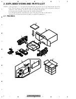
Page 8: ...ts indicates the importance of the safety factor of the part Therefore when replacing be sure to use parts of identical designation Screw adjacent to mark on the product are used for disassembly For the applying amount of lubricants or glue follow the instructions in this manual In the case of no amount instructions apply as you think it appropriate DEH P40MP XU EW5packing 20 16 2 19 18 17 13 6 15...

Page 9: ...lyethylene Bag CEG 127 11 Screw CRZ50P090FTC 12 Screw TRZ50P080FTC 13 Polyethylene Bag CEG1160 14 Handle CND3707 15 Bush CNV3930 16 Carton YHG5142 17 Contain Box YHL5142 18 Protector YHP5008 19 Protector YHP5009 20 1 Owner s Manual YRD5110 20 2 Owner s Manual YRD5111 20 3 Owner s Manual YRD5112 20 4 Installation Manual YRD5113 20 5 Warranty Card CRY1157 Mark No Description Part No Part No Language...

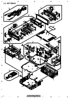
Page 10: ...75 76 67 46 54 56 55 68 52 45 47 62 61 66 65 63 57 60 58 48 59 49 53 53 73 64 44 43 15 42 42 42 32 35 38 37 39 34 41 40 33 36 31 44 44 44 74 12 7 5 2 26 27 17 20 25 21 22 28 71 72 70 70 23 24 11 10 8 9 13 4 4 4 6 69 18 3 1 1 1 1 18 18 16 14 29 30 19 17 51 51 50 DEH P40MP XU EW5 ...

Page 11: ...ETACH CAC4836 33 Spring CBH1835 34 Spring CBH2208 35 Spring CBH2367 36 Bracket CNC6791 37 Holder CNC8042 38 Cover CNM6276 39 Arm CNV4692 40 Arm CNV4728 41 Arm CNV5576 42 Screw IMS20P030FTB 43 Detachable Assy YXA5220 44 Screw BPZ20P080FTB 45 Spring CBH2210 46 Knob SOURCE VOLUME YAA5008 47 Button 1 6 YAC5074 48 Button EQ BAND ESC YAC5075 49 Button ATT DISP SCRL YAC5076 50 Button TA EJECT YAC5077 51 ...

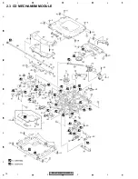
Page 12: ...DEH P40MP XU EW5 12 1 2 3 4 1 2 3 4 C D F A B E 2 3 CD MECHANISM MODULE ...

Page 13: ...CND2584 30 Lever CND2585 31 Arm CND2586 32 Bracket CND2587 33 Arm CND2588 34 Lever CND2589 35 Holder CNV7201 36 Gear CNV7207 37 Gear CNV7208 38 Gear CNV7209 39 Gear CNV7210 40 Gear CNV7211 41 Gear CNV7212 42 Rack CNV7214 43 Arm CNV7216 44 Roller CNV8189 45 Gear CNV7219 46 Guide CNV7361 47 Gear CNV7595 48 Guide CNV8448 49 Arm CNV7805 50 Rack CNV8342 51 Roller CNV8343 52 Holder CNV8344 53 Arm CNV834...

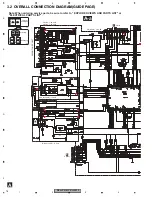
Page 14: ...LOEJ 5 52 50 X201 XTAL XTAL 16 93MHz VDSENS 11 VD IN2_L IN4 _ IN4 _ IN1_L 2 5 4 ELEC SOU TUNL 1 SYSTEM CON IC601 2 PEG28 CN401 1 2 CN701 CN101 TUNER AMP UNIT LOUT A CN621 T VDD_3 3V VCC8 VDD5 T C T ANTENNA C TUNPDI TUNPCK TUNPDO 13 9 KEY2 KEY1 KEYAD 94 KEYD 34 RX RX2 TX ASENBO IPPW 29 30 40 27 52 IP_BUS Q101 Q102 B UP IN1 B14 7 IN1 11 6 1 5 IC101 HA12241FP 2 1 8 5 8 2 3 B UP 5 Q702 VD 1 2 Q701 BRS...

Page 15: ...DL1 33 CE2 TUNPCE2 B UP B UP 20 6 48 SYSPW 25 1 2 1 3 4 B REM RESET BSENS ASENS VCC8 6 SSENS VDD5 Q852 B UP Q841 SWVDD 7 18 ILMPW 1 DSENS Q842 SWVDD DSENS ILMB ROT1 ROT0 DPDT KYDT SRC DSENS ILM ROT1 ROT0 DPDT KYDT IC 1801 PD6340A LCD DRIVER KEY CONTROLLER KEY DATA LCD1801 8 CN1801 KEYBOARD UNIT 5 4 18 20 DPDT KYDT B 3 2 D1804 D1822 SWVDD SWVDD 7 XO XI 22 X1801 5MHz 23 KEY MATRIX TA S1814 DISP S181...

Page 16: ...A a A b A b A b A b A a A a Large size SCH diagram Guide page Detailed page Note When ordering service parts be sure to refer to EXPLODED VIEWS AND PARTS LIST or ELECTRICAL PARTS LIST C CN701 FM AM TUNER UNIT B CN1801 15MHz CSS1653 CD 20 dB 19 4 dB FM 10 29 5 dB AM 15 26 0 dB AUX IN 20 dB 17 8 dB IP BUS 20 dB 17 8 dB ...

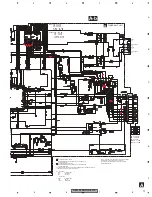
Page 17: ...ue 103 0 01uF 101 10 100uF 10V The mark found on some component parts indicates the importance of the safety factor of the part Therefore when replacing be sure to use parts of identical designation Symbol indicates a resistor No differentiation is made between chip resistors and discrete resistors NOTE Symbol indicates a capacitor No differentiation is made between chip capacitors and discrete ca...

Page 18: ... a A b A b 1 2 600µH 3300 16 CEK1208 10A SUB WOOFER R CH FRONT R CH FRONT L CH SUB WOOFER L CH G A TUNER AMP UNIT 3A INPUT FM 33 1 dB AM 29 6 dB CD 22 4 dB IP BUS 20 8 dB AUX IN 20 8 dB OUTPUT FM 12 0 dB AM 8 5 dB CD 8 3 dB IP BUS 8 7 dB AUX IN 8 7 dB ...

Page 19: ...ms Capacitors Code Practical value 103 0 01uF 101 10 100uF 10V The mark found on some component parts indicates the importance of the safety factor of the part Therefore when replacing be sure to use parts of identical designation Symbol indicates a resistor No differentiation is made between chip resistors and discrete resistors NOTE Symbol indicates a capacitor No differentiation is made between...

Page 20: ...DEH P40MP XU EW5 20 1 2 3 4 1 2 3 4 C D F A B E A b A a A a A b 1 2 C CN701 FM AM TUNER UNIT 15MHz CSS1653 CD 20 dB 19 4 dB FM 10 29 5 dB AM 15 26 0 dB AUX IN 20 dB 17 8 dB ...

Page 21: ...DEH P40MP XU EW5 21 5 6 7 8 5 6 7 8 C D F A B E A a A b A b A a 3 4 5 6 B CN1801 AUX IN 20 dB 17 8 dB IP BUS 20 dB 17 8 dB ...

Page 22: ...DEH P40MP XU EW5 22 1 2 3 4 1 2 3 4 C D F A B E 3 3 KEYBOARD UNIT B LCD DRIVER KEY CONTROLLER ...

Page 23: ...DEH P40MP XU EW5 23 5 6 7 8 5 6 7 8 C D F A B E B A CN804 B KEYBOARD UNIT ...

Page 24: ...OR M2 CXC4026 LOADING CARRIAGE MOTOR PICKUP UNIT P10 5 SERVICE SWITCHES CD CORE UNIT S10 5COMP2 S901 HOME SWITCH ON OFF S903 DSCSNS SWITCH ON OFF S904 12EJ SWITCH ON OFF S905 8EJ SWITCH ON OFF The underlined indicates the switch position CD DRIVER F F T T F F T T F F T T F F T T F T S C C S S C 3 2 1 9 0 4 8 7 5 ...

Page 25: ...DEH P40MP XU EW5 25 5 6 7 8 5 6 7 8 C D F A B E C b C C CD CORE UNIT S10 5COMP2 A CN701 F SIGNAL LINE FOCUS SERVO LINE TRACKING SERVO LINE CARRIAGE SERVO LINE SPINDLE SERVO LINE T C S 6 ...

Page 26: ...DEH P40MP XU EW5 26 1 2 3 4 1 2 3 4 C D F A B E C a C b C b 1 C CD CORE UNIT S10 5COMP2 F SIGNAL LINE FOCUS SERVO LINE TRACKING SERVO LINE CARRIAGE SERVO LINE SPINDLE SERVO LINE T C S ...

Page 27: ...DEH P40MP XU EW5 27 5 6 7 8 5 6 7 8 C D F A B E C a C b C b 2 3 A CN701 6 ...

Page 28: ...4 1 2 3 4 C D F A B E C b C a C a C b 1 PICKUP UNIT P10 5 SERVICE SWITCHES CD CORE UNIT S10 5COMP2 S901 HOME SWITCH ON OFF S903 DSCSNS SWITCH ON OFF S904 12EJ SWITCH ON OFF S905 8EJ SWITCH ON OFF F F T T F F T T F F T T F F T T ...

Page 29: ...XC7134 SPINDLE MOTOR M2 CXC4026 LOADING CARRIAGE MOTOR SWITCHES CD CORE UNIT S10 5COMP2 S901 HOME SWITCH ON OFF S903 DSCSNS SWITCH ON OFF S904 12EJ SWITCH ON OFF S905 8EJ SWITCH ON OFF The underlined indicates the switch position CD DRIVER F T S C C S S C 3 2 1 9 0 4 8 7 5 ...

Page 30: ...500 mV div 500 mV div 500 mV div 500 mV div 20 ms div FE 0FIN TE 9TIN 1 V div 500 mV div 500 mV div 500 μs div RFAGC TE 9TIN 500 mV div 500 mV div 2 ms div TE RFAGC 500 mV div 500 mV div 200 ms div 0FIN FE Source On setup operation 12 cm CD DA Source On setup operation CD DA Play operation Spindle waveform during play operation Spindle waveform during play operation Wider Focus Search waveform Tra...

Page 31: ...1 V div 1 V div 1 V div 500 μs div RFAGC 9TIN TE 0FIN 5 V div 5 V div 5 V div 5 V div 500 ms div 1DSCSNS 28SNS 312SNS 4LOEJ 5 V div 5 V div 5 V div 500 ms div 1DSCSNS 5CLCONT 4LOEJ 12 cm CD Eject operation Analog audio waveform 12 cm CD Eject operation 8 cm CD Eject operation Black dot 800 μm during play Search operation Outter to Inner 4 Tracks Jump waveform 10 Tracks Jump waveform 32 Tracks Jump...

Page 32: ...tor P C Board Chip Part SIDE B SIDE A NOTE FOR PCB DIAGRAMS 1 The parts mounted on this PCB include all necessary parts for several destination For further information for respective destinations be sure to check with the schematic dia gram 2 Viewpoint of PCB diagrams C CN701 AUX WIRED REMOTE INPUT IP BUS INPUT CORD ASSY DSENS ...

Page 33: ...DEH P40MP XU EW5 33 5 6 7 8 5 6 7 8 C D F A B E A SIDE A 4 3 2 1 G G G G B CN1801 FRONT FM AM TUNER UNIT FRONT OUTPUT REAR OUTPUT OR SUBWOOFER OUTPUT ANTENNA ...

Page 34: ...DEH P40MP XU EW5 34 1 2 3 4 1 2 3 4 C D F A B E A A TUNER AMP UNIT 1 TEST FU353 B 131 131 Fuse 3 A CEK1286 ...

Page 35: ...DEH P40MP XU EW5 35 5 6 7 8 5 6 7 8 C D F A B E A SIDE B PCL ...

Page 36: ...DEH P40MP XU EW5 36 1 2 3 4 1 2 3 4 C D F A B E 4 2 KEYBOARD UNIT B SIDE B SIDE A B KEYBOARD UNIT B KEYBOARD UNIT A CN804 EJECT AUDIO DISPLAY SOURCE VOLUME EQ BAND ATT FUNCTION 1 2 3 4 5 6 TA ...

Page 37: ...DEH P40MP XU EW5 37 5 6 7 8 5 6 7 8 C D F A B E ...

Page 38: ...DEH P40MP XU EW5 38 1 2 3 4 1 2 3 4 C D F A B E 4 3 CD CORE UNIT S10 5COMP2 C SIDE A C CD CORE UNIT S10 5COMP2 PICKUP UNIT P10 5 SERVICE A CN701 M2 LOADING CARRIAGE MOTOR M1 SPINDLE MOTOR ...

Page 39: ...DEH P40MP XU EW5 39 5 6 7 8 5 6 7 8 C D F A B E C SIDE B C CD CORE UNIT S10 5COMP2 ...

Page 40: ...ansistor UMH1N Q 451 B 121 110 Transistor DTC124EUA Q 453 B 121 116 Transistor UMD2N Q 701 B 25 49 Transistor UMD2N Q 702 A 6 65 Transistor 2SD2396 Q 841 B 125 24 Transistor 2SA1036K Q 842 B 120 26 Transistor DTC114EUA Q 851 B 36 11 Transistor 2SA1036K Q 852 B 36 7 Transistor DTC114EUA Q 911 A 6 99 Transistor 2SD2396 Q 912 B 18 68 Transistor UMD2N Q 931 B 61 86 Transistor UMX1N Q 951 B 81 87 Trans...

Page 41: ...RS1 16S221J R 453 B 121 113 RS1 16S153J R 454 A 117 113 RD1 4PU102J R 602 B 68 42 RS1 16S103J R 603 B 98 83 RS1 16S103J Circuit Symbol and No Part No R 604 B 97 62 RS1 16S681J R 605 B 153 59 RS1 16S681J R 606 B 110 40 RS1 16S103J R 607 B 145 56 RS1 16S681J R 610 B 104 50 RS1 16S473J R 613 B 98 75 RS1 16S104J R 615 B 69 62 RS1 16S0R0J R 616 B 36 48 RS1 16S473J R 619 B 112 51 RS1 16S0R0J R 620 B 93 ...

Page 42: ...9 CEJQ220M10 C 412 B 160 40 CKSRYB105K10 C 451 A 120 121 CEJQ330M10 C 601 B 73 41 CCSRCH180J50 C 602 B 78 41 CCSRCH180J50 Circuit Symbol and No Part No C 604 B 94 42 CKSRYB105K10 C 605 A 97 40 CEJQ100M16 C 606 B 79 32 CKSRYB104K25 C 607 A 71 29 CEJQ100M16 C 609 B 146 48 CCSRCH470J50 C 701 B 23 44 CKSRYB473K25 C 703 A 30 27 CEJQ101M10 C 704 B 144 73 CKSRYB105K10 C 705 B 126 74 CKSRYB105K10 C 708 A ...

Page 43: ...6 72 Transistor 2SA1577 Q 102 B 47 57 Transistor 2SB1689 X 201 A 23 35 Ceramic Resonator 16 934 MHz CSS1603 S 901 A 53 37 Switch HOME CSN1067 Circuit Symbol and No Part No S 903 B 19 58 Switch DSCSNS CSN1067 S 904 B 38 67 Switch 12EJ CSN1068 S 905 B 24 68 Switch 8EJ CSN1068 RESISTORS R 101 B 60 73 RS1 10SR2R4J R 102 B 59 71 RS1 10SR2R4J R 103 B 60 71 RS1 10SR2R7J R 104 B 52 69 RS1 16SS222J R 105 B...

Page 44: ...39 62 CKSSYB103K16 C 229 B 49 59 CKSSYB104K10 C 236 A 42 61 CKSSYB104K10 C 239 B 44 51 CCSSCH220J50 C 240 A 35 61 CKSSYB104K10 C 250 B 36 30 CKSSYB102K50 C 251 B 33 29 CKSSYB102K50 C 303 A 35 19 CKSSYB472K25 C 304 A 34 21 CKSSYB223K16 C 307 B 25 9 CKSRYB104K16 C 308 B 10 27 CKSRYB105K10 C 703 B 11 37 CCSSCH101J50 C 704 B 8 36 CKSSYB102K50 C 711 A 25 26 CKSSYB104K10 Miscellaneous Parts List Pickup ...

Page 45: ...re protections will not work Avoid applying any mechanical or electrical shock to the mechanism during adjustment The RFI and RFO signals with a wide frequency range are easy to oscillate When observing the signals insert a resistor of 1k ohms in series The load and eject operation is not guarantied with the mechanism upside down If the mechanism is blocked due to mistaken eject operation reset th...

Page 46: ...e S Curve Rough Servo and RF AGC F T RF AGC 4 SPDL 1X 2X switching As for the double speed 2x audio output cannot be supported 5 Error Rate measurement ON ERR 30Counts Start BER display data 6 F Mode switching Tracking Close CRG TR Jump Switching After the Eject key is pressed keys other than the Eject key should not be pressed until disc ejection is complete When the key 2 or 3 is pressed during ...

Page 47: ...de load the disc and switch the 3 V regulator on 2 Using the and buttons move the PU unit to the innermost track 3 Press key 3 to close focus the display should read 91 Press key 2 to implement the tracking balance adjustment the display should now read 81 Press key 3 The display will change returning to 81 on the fourth press 4 As shown in the diagram above monitor the LPF outputs using the oscil...

Page 48: ...DEH P40MP XU EW5 48 1 2 3 4 1 2 3 4 C D F A B E Grating waveform 45 0 75 60 30 90 Ech Xch 20 mV div AC Fch Ych 20 mV div AC ...

Page 49: ... or CRG move mechanism Communication error between microcomputer and SERVO LSI 11 Electricity Focus Servo NG Focusing not available Stains on rear side of disc or excessive vibrations on REWRITABLE 12 Electricity Spindle Lock NG Spindle not locked Sub code is strange not readable Subcode NG Failure on spindle stains or damages on disc or excessive vibrations A disc not containing CD R data is foun...

Page 50: ...itched ON the standby mode cancelled shift the TESTIN IC601 Pin 88 terminal to H The clock signal is output from the PCL terminal IC601 Pin 39 The frequency of the clock signal is 468 750 Hz that is one 32th of the fundamental frequency The clock signal should be 468 750 Hz 10 Hz 15 Hz If the clock signal is out of the range the X tal X601 should be replaced with new one ...

Page 51: ...ig 1 Removing the Tuner Amp Unit Fig 2 Grille Assy Remove the four screws 1 Remove the Case Remove the screw Remove the three screws Straighten the tabs at four locations indicated and then remove the Tuner Amp Unit 2 1 2 1 2 1 1 2 3 1 3 3 3 2 Disconnect the connector and then remove the CD Mechanism Module Tuner Amp Unit 2 Release the two latchs and then remove the Grille Assy Removing the Case n...

Page 52: ...the mechanism remove the two Springs A the six Springs B and the four Screws 2 Turn the Upper Frame using the part a as a pivot and remove the Upper Frame 3 While lifting the Carriage Mechanism remove it from the three Dampers Caution When assembling be sure to apply some alcohol to the Dampers and assemble the mechanism in a clamped state 1 Hold the Upper and Lower Frames 2 Do not hold the front ...

Page 53: ...the SW in a clamped state so as not to damage it How to remove the Pickup Unit 1 Make the system in the carriage mechanism mode and have it clamped 2 Remove the CD Core Unit and remove the leads from the Inner Holder 3 Remove the Poly Washer Change Arm and Pickup Lock Arm 4 While releasing from the hook of the Inner Holder lift the end of the Feed Screw Caution When assembling move the Planet Gear...

Page 54: ...4 NC 5 BUS 6 GND 7 BUS L 8 ASENB 9 BUS R 10 BUS R 11 BUS L 11 10 9 8 7 6 5 4 3 2 1 IP BUS INPUT ANTENNA AUX REAR OUTPUT OR SUBWOOFER OUTPUT FRONT OUTPUT 16 15 14 13 12 11 10 9 8 7 6 5 4 3 2 1 1 B UP 2 GND 3 ACC 4 NC 5 NC 6 B REM 7 NC 8 TEL 9 RL 10 FL 11 RL 12 FL 13 RR 14 FR 15 RR 16 FR WIRED REMOTE INPUT ...

Page 55: ...TBY 5 OUT2 6 VCC 7 OUT1 8 P GND1 9 OUT1 10 SVR 11 IN1 12 IN2 13 S GND 14 IN4 15 IN3 16 AC GND 17 OUT3 18 P GND3 19 OUT3 20 VCC 21 OUT4 22 MUTE 23 OUT4 24 P GND4 SWITCH 25 Offset Detection Offset Detection Offset Detection Offset Detection Protector Over current limit sw_vcc stby Protector Short circuit Mute circuit amp_vcc Stand by Circuit Protector Over voltage sw_vcc Protector Thermal Reference ...

Page 56: ...m Isolator Isolator Auto Zero Gain Adjuster Input Selector TRE BASS LOUDNESS Front_R Rear_R Front_L Rear_L Anti Alias Filter Primary Volume IN1_L IN2_L IN3_L IN4 _L IN4 _L IN4 _R IN4 _R IN3_R IN2_R IN1_R STB DATA CLK GND Vcc Vref MID Level Meter LM_out Secondary Volume Secondary Volume Pre SW_L Pre SW_R Anti Radiation Filter Supply Reference Anti Radiation Filter HPF Digital Block Phase inv LPF FI...

Page 57: ...DEH P40MP XU EW5 57 5 6 7 8 5 6 7 8 C D F A B E NJM2794V OUT2 OUT1 IN1 IN1 IN2 IN2 Vref GND V 14 13 12 11 10 9 8 1 2 3 4 5 6 7 IN1 NC IN1 NC IN2 NC IN2 OUT1 NC GND VREF V NC OUT2 ...

Page 58: ...sor mode change input Not used Reset input Main clock output GND Main clock input Power supply input NMI input Detach sense input Backup sense input ACC sense input CD mechanism RESET output VD power supply output P BUS Reset output P BUS Reception enable input output P BUS Service request input Not used IPBUS Input 2 Not used IPBUS Input IPBUS Output PBUS Output PBUS Input PBUS Clock output Wired...

Page 59: ...I I O O I I I I Format C C C C C C C TUNER Chip enable output PLL TUNER Clock output PLL TUNER Data input PLL Not used RDS Clock interrupt RDS PLL lock detection interrupt Not used RDS Lock signal input RDS Data input RDS57K input connected to HSLK Not used For operation check of RDS circuit TUNER Data output PLL Not used Test program input Not used Source key Not used Wired remote control AD inpu...

Page 60: ...0 O Key strobe output 15 16 KDT0 1 I Key data input analogue input 17 REM I Remote control reception input 18 DPDT I Display data input 19 NC Not used 20 KYDT O Key data output 21 MODA GND 22 X0 Crystal oscillator connection pin 23 X1 Crystal oscillator connection pin 24 VSS GND 25 26 KDT2 3 I Key data input 27 NC Not used 28 KST4 O Key strobe output 29 32 NC Not used 33 55 SEG35 13 O LCD segment ...

Page 61: ...ower supply for A D converter Ground for A D converter Flash writing control terminal Internal microcomputer reset terminal Pull down Not used Chip check test program start up input Not used P BUS Serial data input P BUS Serial data output P BUS Serial clock input output Tx for flash rewriting Rx for flash rewriting P BUS Reception enable input output P BUS Service request input Not used Flash sel...

Page 62: ...udio serial I F clock output 3 wire audio serial I F data output Servo monitor input output 0 2 Servo monitor input output 3 Ext MCK IN DRAM CLOCK DRAM CS DRAM CKE output Output of DRAM RAS DRAM Lower CAS LDQM output DRAM Upper CAS UDQM output Output of DRAM WE DRAM OE CAS output Input output of DRAM data 0 15 Ground for I O terminal Power supply for I O terminal Output of DRAM address 0 11 Output...

Page 63: ... 13 is connected with a power supply of micro computer 14 DO O data out Data output 15 DGND digital ground Ground of digital block 16 NC non connection Not used 17 VDD_3 3 power supply The power supply for digital block 3 3 V 0 2 V 18 RDS_CK O RDS clock Output of RDS clock 2 5 V 19 RDS_DATA O RDS data Output of RDS data 2 5 V 20 RDS_LOCK O RDS lock Output unit High active 2 5 V RDS_LOCK turns over...

Page 64: ...DEH P40MP XU EW5 64 1 2 3 4 1 2 3 4 C D F A B E 7 2 2 DISPLAY LCD YAW5064 SEGMENT COMMON ...

Page 65: ...20 dsens Pin 18 SWVDD H Pin 7 ASENBO H Pin 40 Source keys operative Completes power on operation After that proceed to each source operation SYSPW H Pin 48 Starts communication with Grille microcomputer Source ON 300 ms 300 ms In case of the above signal the communication with Grille microcomputer may fail If the time interval is not 300 msec the oscillator may be defective ...

Page 66: ...DEH P40MP XU EW5 66 1 2 3 4 1 2 3 4 C D F A B E 8 OPERATIONS ...

Page 67: ...DEH P40MP XU EW5 67 5 6 7 8 5 6 7 8 C D F A B E CBA1994 ...

Page 68: ...DEH P40MP XU EW5 68 1 2 3 4 1 2 3 4 C D F A B E Connection Diagram ...

Page 69: ...DEH P40MP XU EW5 69 5 6 7 8 5 6 7 8 C D F A B E ...

Page 70: ...eaning tools Portions to be cleaned Cleaning tools g CD pickup lenses Cleaning liquid GEM1004 Cleaning paper GED 008 g p p Jigs List Test Disc L P F TCD 782 Checking the grating g g g Checking the grating g g g Two pieces p Name Jig No Remarks Grease List Grease Grease GEM1024 GEM1045 CD Mechanism Module CD Mechanism Module Name Grease No Remarks ...

Reviews: