21
VSX-519V-K
5
6
7
8
5
6
7
8
A
B
C
D
E
F
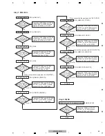
5. DIAGNOSIS
5.1 DIAGNOSIS FLOWCHART
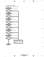
Step 3: Regulator IC
REG101, REG102 (Pin 3)
Is the
voltage of 3.3 V
input?
Replace REG103.
Check the ZD200 2.4 VB
and IC106.
To Step 3
To Step 4
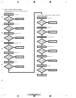
Step 0: Preliminary confirmation
Confirm the following items before checking
Tighten screws securely.
No
Yes
To Step 1
No
Troubleshooting
[1] DSP TROUBLESHOOTING
Step 2: Regulator IC
Check the REG101,
REG102 and MAIN Assy
Check the REG103 and
MAIN Assy.
REG103 (Pin 3)
Is the
voltage of around
5 V input?
No
Yes
(to chassis)
ZD200 kathode
Is the
voltage of 2.5 V
output?
No
*The I/O power of DSP Assy is OK
*The IC106 power of DSP Assy
*the DSP IC CORE power of DSP Assy
XMCK
Note: REG101, REG102 is made of
parallel connection.
REG103 (Pin 2)
Is the
voltage of 3.3 V
output?
No
Yes
Yes
Yes
Is the
voltage of 1.2 V
output?
Replace REG101, 102.
Check the path to XTAL101.
No
Yes
(to chassis)
(to chassis)
REG101, REG102 (Pin 2) (to chassis)
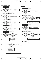
Step 1: BtoB connector
CP200,CN206,CP105
Are the
connectors securely
inserted?
Turn the power off and
insert the connectors
securely.
No
Yes
To Step 2
*CN206,CP200 connectors
doesn't connection in case
of DSP JIG B'D use.
BtoB connector
Do screws of COAX
Jack securely tighten?
OR connect GND wire of
DSP JIG B'D to chassis.
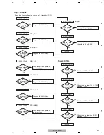
Step 4: X'tal
To Step 5
Yes
IC109 (Pin 6, 7)
No
Is there
a 24.576 MHz
output?
Check the path to pin 6, 7 of IC109.
Replace XTAL101.
Yes
IC102 (Pin 17)
No
Is there
a 24.576 MHz
input?
Summary of Contents for VSX-519V-K
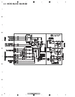
Page 18: ...18 VSX 519V K 1 2 3 4 A B C D E F 1 2 3 4 4 3 VIDEO BLOCK DIAGRAM P C B SUB ASSY VIDEO 519 L ...
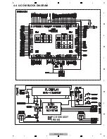
Page 19: ...19 VSX 519V K 5 6 7 8 5 6 7 8 A B C D E F 4 4 U COM BLOCK DIAGRAM P C B SUB ASSY FRONT C ...
Page 45: ...45 VSX 519V K 5 6 7 8 5 6 7 8 A B C D E F ...
Page 57: ...57 VSX 519V K 5 6 7 8 5 6 7 8 A B C D E F J CN401 M CP107 A FL FL FL SL SL SL C C C ...
Page 67: ...67 VSX 519V K 5 6 7 8 5 6 7 8 A B C D E F P 2 2 116 ...
Page 71: ...71 VSX 519V K 5 6 7 8 5 6 7 8 A B C D E F B A SIDE B B P C B SUB ASSY P T ...
Page 77: ...77 VSX 519V K 5 6 7 8 5 6 7 8 A B C D E F J 01 SIDE A SIDE B ...
Page 81: ...81 VSX 519V K 5 6 7 8 5 6 7 8 A B C D E F L SIDE A ...
Page 83: ...83 VSX 519V K 5 6 7 8 5 6 7 8 A B C D E F L SIDE B ...
Page 89: ...89 VSX 519V K 5 6 7 8 5 6 7 8 A B C D E F P N SIDE B ...


