background image

25

VSX-519V-K

5

6

7

8

5

6

7

8

A

B

C

D

E

F

1. Causes for noncompletion of HDMI authentication between the source e

q

uipment and this unit

    (the HDMI indicator is unlit or flashes)

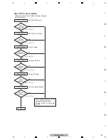
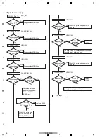
[2] HDMI TROUBLESHOOTING

Causes for no display or sound from the monitor

HDMI Simple Diagnosis

Replace the HDMI cable.

NG

OK

OK

OK

Connect the source equipment 
(player) to the Sink equipment 
(monitor) directly.

Replace the Player.

Replace the HDMI cable.

Repare the Receiver.

Repare the Player.

NG

OK

Replace the Monitor.

Repare the Monitor.

NG

POWER ON

Confirm the following items before checking

Do

screws of COAX

jack securely

tighten?

Tighten screws securely.

No

Yes

Source equipment:
Connect a DVD player to BD, TV or DVR.

To Step 2

To Step 1

Sink equipment:
Connect a TV to HDMI OUT.

Turn on the power of the Receiver and equipments 
which was connected with HDMI.

Function switch (BD, TV or DVR)

Switch the function that HDMI was assigned.
Factory shipments setting:
HDMI 1: BD/DVD
HDMI 2: TV/SAT
HDMI 3: DVR/VCR

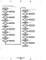
HDMI Troubleshooting

Step 0: Preliminary confirmation

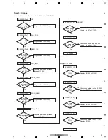
Step 1: Connect the HDMI e

q

uipment

Summary of Contents for VSX-519V-K

Page 1: ... Keetberglaan 1 9120 Melsele Belgium 2009 Printed in Japan VSX 519V K RRV3897 AUDIO VIDEO MULTI CHANNEL RECEIVER VSX 519V K VSX 519V S THIS MANUAL IS APPLICABLE TO THE FOLLOWING MODEL S AND TYPE S Model Type Power Requirement Remarks VSX 519V K MYSXCN5 AC 220 V to 230 V VSX 519V S MYSXCN5 AC 220 V to 230 V For details refer to Important Check Points for good servicing T ZZK MAR ...

Page 2: ...visual inspection nor the protection afforded by them necessarily can be obtained by using replacement components rated for voltage wattage etc Replacement parts which have these special safety characteristics are identified in this Service Manual Electrical components having such features are identified by marking with a on the schematics and on the parts list in this Service Manual The use of a ...

Page 3: ... the product Please check that neither solder debris nor screws remain inside the product 8 There should be no semi broken wires scratches melting etc on the coating of the power cord Damaged power cords may lead to fire accidents so please be sure that there are no damages If you find a damaged power cord please exchange it with a suitable one 9 There should be no spark traces or similar marks on...

Page 4: ...RRENT ADJUSTMENT 44 9 EXPLODED VIEWS AND PARTS LIST 46 9 1 PACKING SECTION 46 9 2 EXTERIOR SECTION 48 10 SCHEMATIC DIAGRAM 52 10 1 P C B SUB ASSY MAIN and P C B SUB ASSY P T 52 10 2 P C B SUB ASSYS FRONT VOLUME FUNCTION HEADPHONE and PORTABLE 54 10 3 P C B SUB ASSY AMP 56 10 4 P C B SUB ASSY INPUT 58 10 5 P C B SUB ASSY VIDEO 519 60 10 6 P C B SUB ASSY SPEAKER 519 and P C B SUB ASSY CNT 62 10 7 P ...

Page 5: ... be set to around 373 ºC in general although the temperature depends on the heat capacity of the PC board on which reworking is required and the weight of the tip of the soldering iron Do NOT use a soldering iron whose tip temperature cannot be controlled Compared with eutectic solders lead free solders have higher bond strengths but slower wetting times and higher melting temperatures hard to mel...

Page 6: ... Active High Level 2 0 V Miscellaneous Power Requirements AC 220 V to 230 V 50 Hz 60 Hz Power Consumption 260 W In standby 0 65 W Dimensions 420 mm W x 158 mm H x 347 7 mm D Weight without package 8 8 kg Furnished Parts Remote control 1 Dry cell batteries AAA size IEC R03 2 AM loop antenna 1 FM wire antenna 1 Power cord 1 Warranty card 1 Operating instructions Note The specifications are applicabl...

Page 7: ...tween Auto surround mode and Stream Direct playback Stream Direct playback bypasses the tone controls for the most accurate reproduction of a source STEREO A L C Switches between stereo playback Auto level control stereo mode and Front Stage Surround Advance modes ADVANCED SURROUND Switches between the various surround modes STANDARD SURROUND Press for Standard decoding and to switch between the v...

Page 8: ...adio station is registered 10 PRESET information or input signal indicator Shows the preset number of the tuner or the input signal type etc 11 DTS indicators DTS Lights when a source with DTS encoded audio signals is detected 96 24 Lights when a source with DTS 96 24 encoded audio signals is detected 12 Character display Displays various system information 13 Dolby Digital indicators Lights when ...

Page 9: ... Press to restore CD quality sound to compressed audio sources Press BD first to access BD MENU Displays the disc menu of Blu ray Discs 7 Listening mode buttons AUTO DIRECT Switches between Auto surround mode and Stream Direct playback Stream Direct playback bypasses the tone controls for the most accurate reproduction of a source STEREO A L C Switches between stereo playback Auto level control st...

Page 10: ... VCR These buttons switch between the hard disk DVD and VCR controls for HDD DVD VCR recorders TEST TONE Outputs the test tones on each channel Use the buttons to select the channel and use the buttons to adjust the level on each channel Pressing TEST TONE again exits the test tone mode CH SELECT Press repeatedly to select a channel then use to adjust the level CH SELECT Use to adjust the channel ...

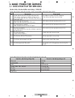
Page 11: ...e the analog connections with a DVD player Each channel audio and operations must be normal Check the digital audio playback Make the digital connections with a DVD player Each channel audio and operations must be normal Check surround playback Select Surround mode and check the multichannel operations via the DSP circuit Each channel audio and operations must be normal Check the tuner AM and FM o...

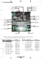
Page 12: ...SY FRONT 7025HK0812011 IL 2 P C B SUB ASSY FRONT 7028067511020 IL 2 P C B SUB ASSY HEADPHONE 7028067512010 IL 2 P C B SUB ASSY VOLUME 7028067513010 IL 2 P C B SUB ASSY FUNCTION 7028067514010 IL 2 P C B SUB ASSY PORTABLE 7028067518010 IL NSP 1 P C B TOTAL ASSY INPUT 7025HK0812013 IL 2 P C B SUB ASSY INPUT 7028067531020 IL NSP 1 P C B TOTAL ASSY VIDEO 519 7025HK0812014 IL 2 P C B SUB ASSY VIDEO 519 ...

Page 13: ...icon adhesive Name Lubricants and Glues No Remarks Refer to 9 2 EXTERIOR SECTION Refer to 9 2 EXTERIOR SECTION Lubricants and Glues list Name Jig No Remarks 10P extension jig cable GGD1628 Diagnosis 8P extension jig cable GGD1629 Diagnosis Board to board extension jig cable GGD1630 Diagnosis Jigs list ...

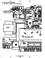
Page 14: ...1 OVERALL CONNECTION DIAGRAM P C B SUB ASSY L P 7 P C B SUB ASSY FUNCTION 7028067514010 IL E E P C B SUB ASSY HEADPHONE 7028067512010 IL F F P C B SUB ASSY SPEAKER 519 7028067601030 IL M P C B SUB ASSY 7028067501020 IL A P C B SUB ASSY AMP 7028067521010 IL J P A ...

Page 15: ...IL C P C B SUB ASSY VOLUME 7028067513010 IL D P C B SUB ASSY CNT 7028067504010 IL N P C B SUB ASSY INPUT 7028067531020 IL K P C B SUB ASSY HDMI 519 7028067581010 IL Q P 1 2 2 2 P C B SUB ASSY DSP 7028067561020 IL SUB ASSY MAIN 67501020 IL P C B SUB ASSY P T 7028067505010 IL B P C B SUB ASSY PORTABLE 7028067518010 IL I ...

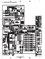
Page 16: ...16 VSX 519V K 1 2 3 4 A B C D E F 1 2 3 4 4 2 AUDIO BLOCK DIAGRAM I P C B SUB ASSY HDMI 519 Q P C B SUB ASSY DSP P C B SUB ASSY MAIN A P K P C B SUB PORTABL ...

Page 17: ...17 VSX 519V K 5 6 7 8 5 6 7 8 A B C D E F P C B SUB ASSY HEADPHONE F I P C B SUB ASSY INPUT P C B SUB ASSY AMP J P C B SUB ASSY SPEAKER 519 M K P C B SUB ASSY PORTABLE ...

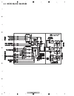
Page 18: ...18 VSX 519V K 1 2 3 4 A B C D E F 1 2 3 4 4 3 VIDEO BLOCK DIAGRAM P C B SUB ASSY VIDEO 519 L ...

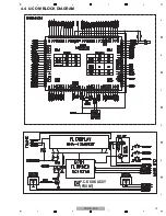
Page 19: ...19 VSX 519V K 5 6 7 8 5 6 7 8 A B C D E F 4 4 U COM BLOCK DIAGRAM P C B SUB ASSY FRONT C ...

Page 20: ...20 VSX 519V K 1 2 3 4 A B C D E F 1 2 3 4 4 5 POWER SUPPLY BLOCK DIAGRAM S4 FLT S3 DSP HDMI AC CORD S2 12V 12V S1 AMP B B S4 DIR CODEC HDMI USB MAIN TRANS SUB TRANS ...

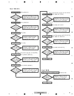
Page 21: ...s OK The IC106 power of DSP Assy the DSP IC CORE power of DSP Assy XMCK Note REG101 REG102 is made of parallel connection REG103 Pin 2 Is the voltage of 3 3 V output No Yes Yes Yes Is the voltage of 1 2 V output Replace REG101 102 Check the path to XTAL101 No Yes to chassis to chassis REG101 REG102 Pin 2 to chassis Step 1 BtoB connector CP200 CN206 CP105 Are the connectors securely inserted Turn t...

Page 22: ...OPT1 Check that the S PDIF signal is output Check that changes by pulling out and inserting the digital input lines Can observe the digital signal No 0 V 3 3 V Yes IC109 Pin 67 COAX Can observe the digital signal No Yes Yes Check that the data and clock signals are output Check that it changes in the Playback and Pause modes of the USB iPod 0 V 3 3 V 0 V 3 3 V 0 V 3 3 V Yes IC109 Pin 71 From USB A...

Page 23: ... and data address lines SDRAM IC100 FLASH ROM IC101 IC109 Pin 25 Surround back L R data No Is there a data input Yes IC109 Pin 27 Surround L R data No IIs there a data input Yes IC109 Pin 18 DSP_BCK Bit clock No Is there a bit clock input Yes IC109 Pin 19 DSP_LRCK LR clock No Is there a LR clock output Yes IC109 Pin 28 Front L R data No Is there a data input 0 V 3 3 V 0 V 3 3 V 0 V 3 3 V 0 V 3 3 V...

Page 24: ... Is the output 2 5 V fixing Analog output of each CH when inputting the digital signal dB no signal Replace IC109 Yes IC109 Pin 43 Surround L out No Is there a audio signal output Replace IC109 Yes IC109 Pin 41 Center out No Is there a audio signal output Replace IC109 Yes IC109 Pin 39 LFE out No Is there a audio signal output Step 7 Codec output analog Analog output of each CH when inputting the ...

Page 25: ...e the Receiver Repare the Player NG OK Replace the Monitor Repare the Monitor NG POWER ON Confirm the following items before checking Do screws of COAX jack securely tighten Tighten screws securely No Yes Source equipment Connect a DVD player to BD TV or DVR To Step 2 To Step 1 Sink equipment Connect a TV to HDMI OUT Turn on the power of the Receiver and equipments which was connected with HDMI Fu...

Page 26: ... 8 V Is the voltage 3 3 V Is the voltage 1 2 V replace IC1005 replace IC1004 IC1005 Pin 3 No HDMI 3 3V Yes IC1005 Pin 2 No HDMI 1 8V Yes Check the parts and patterns in the path Check the parts and patterns in the path Is IC1005 abnormally hot Is IC1004 abnormally hot No Yes IC1004 Pin 3 No HDMI 3 3V HDMI 1 2V Yes The output and GND may be short circuited Check the path between them Check the part...

Page 27: ... Check the parts and patterns in the path pin 89 of IC1003 Step 3 Diagnosis CN1002 Pin 6 Is the voltage 0 to 3 3 V No CE Diagnose the MAIN Assy Diagnose the MAIN Assy Diagnose the MAIN Assy Diagnose the MAIN Assy Diagnose the MAIN Assy Yes CN1002 Pin 7 Is the voltage 0 to 3 3 V No SUB_PDN CN1002 Pin 3 Is there a data input 0 to 3 3 V Is there a data input 0 to 3 3 V No CSCK_MAIN Yes Yes CN1002 Pin...

Page 28: ...he equipment to IN3 DVR VCR Is the voltage 5 V when selecting IN2 Is the voltage 5 V when selecting IN3 JACK1003 Pin 18 5V_R3 Is the voltage 5 V Is the voltage 5 V Is the voltage 5 V Is the voltage 5 V Check the JACK1003 If JACK 1003 is failure replace JACK1003 Check the JACK1001 If JACK 1001 is failure replace JACK1001 Check the JACK1002 If JACK 1002 is failure replace JACK1002 Yes JACK1002 Pin 1...

Page 29: ...1001 and JACK1001 If IC1001 or JACK1001 is failure replace IC1001 or JACK1001 0 to 5 V 0 to 5 V To Step 8 IC1002 Pin 47 SDA HDMI OUT SDA HDMI IN1 BD DVD Does a signal output in constant period 0 to 5 V Check the JACK1004 and IC1002 If JACK1004 or IC1002 is failure replace JACK1004 or IC1002 No No No Yes IC1002 Pin 46 SCL HDMI OUT Does a clock output in constant period 0 to 5 V Check the JACK1004 a...

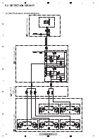
Page 30: ...30 VSX 519V K 1 2 3 4 A B C D E F 1 2 3 4 5 2 DETECTION CIRCUIT 1 DC Protection Circuit Diagram P C B SUB ASSY MAIN A P C B SUB ASSY SPEAKER M P C B SUB ASSY P T B P C B SUB ASSY AMP J ...

Page 31: ...31 VSX 519V K 5 6 7 8 5 6 7 8 A B C D E F 2 Overload Protection Circuit Diagram P C B SUB ASSY MAIN A P C B SUB ASSY P T B P C B SUB ASSY AMP J ...

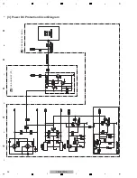
Page 32: ...32 VSX 519V K 1 2 3 4 A B C D E F 1 2 3 4 3 Power DC Protection Circuit Diagram P C B SUB ASSY MAIN A P C B SUB ASSY P T B ...

Page 33: ...er of OVERLOAD error detections Number of abnormal temperature error detections Time sec The numbers of detections for various protection processes are displayed 1 5 normal denotes that the display will return to the normal indication when no key operation is performed for 5 seconds 2 Variable range 0 255 How to enter exit During Standby mode simultaneously press and hold the PRESET and STANDBY ON...

Page 34: ...f protection detections are completed all the counters will be reset to 000 2 Prohibitions The protection detection counts cannot be cleared reset to 000 with the MEMORY CLEAR process They can only be cleared when the procedures of Reset mode are completed 1 5 normal denotes that the display will return to the normal indication when no key operation is performed for 5 seconds 2 Indication when the...

Page 35: ...see 3 4 How to cancel the status after detection of a DC error below A key input will not be inhibited after an OVERLOAD TEMP error is detected The unit can be turned ON Simultaneously holding the ADVANCD SURROUND and STANDBY ON keys on the front panel pressed for 2 seconds will cancel Key Input Inhibition mode after a DC error detection and turn the unit ON Detailed explanations FL Display Descri...

Page 36: ...edures 1 Unplug the power cord 2 Connect CP704 30 V Pins 1 and 2 of the P C B SUB Assy FRONT and GND Pins 3 and 4 respectively using resistor leads with 47 100 ohms 2 W or higher for discharging Discharging time 5 10 seconds depending on the level of resistance 3 Check that the voltage between the 30 V and GND terminals is less than 1 V using a tester Be sure to connect the GND terminal of the tes...

Page 37: ...88 of the P C B SUB Assy DSP may be damaged Note 1 During repair before checking the P C B SUB Assy MAIN etc with the rear chassis removed be sure to connect the GND terminal of the main capacitor to the rear chassis TUNER PACK CHASSIS as shown below then connect the power cord Without grounding connection the protection circuit will be activated After repairing be sure to remove the ground wire b...

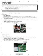
Page 38: ...ving the 10 screws 1 Remove the five screws BBZ30P080FTB 2 Remove the two screws BBZ30P080FTC 3 Remove the two screws 4 Unhook the two hooks 5 Arrange the front panel section as shown in the photo below 1 1 2 2 1 1 3 4 4 3 1 5 Front panel section Bottom view P C B SUB Assy GUIDE PCB L P C B SUB Assy GUIDE PCB R ...

Page 39: ...screws BBZ30P080FTC 3 Disconnect the two connectors 1 1 1 1 1 1 1 Bottom view 2 Remove the four screws BBZ30P080FTC 2 3 3 2 2 2 CP801 CP107 P C B SUB Assy INPUT 819 P C B SUB Assy AMP P C B SUB Assy MAIN Caution Heat sink section in work becomes hot and be careful with it P C B SUB Assy GUIDE PCB L P C B SUB Assy GUIDE PCB R ...

Page 40: ... direction of the arrow 4 5 10P extension jig cable GGD1628 Heat sink section P C B SUB Assy AMP Note The Power transistor and heat sink on the P C B SUB Assy MAIN come closer Make sure that they will not come into contact Heat sink 4 8P extension jig cable GGD1629 Heat sink section Power transistor P C B SUB Assy MAIN ...

Page 41: ... Remove the five screws BBT30P100FTB 1 1 1 1 1 2 3 3 3 3 3 3 2 2 Rear view 2 Remove the three screws BBZ30P080FTC 3 Remove the six screws BBZ30P180FTC 4 Arrange the unit as shown in the photo below 5 Connect the chassis ground See 2 Notes on Ground Points Connection P C B SUB Assy MAIN P C B SUB Assy MAIN 4 5 ...

Page 42: ...e bonnet by removing the 10 screws 1 Remove the three screws B020930083B10 IL 2 Remove the 18 screws BBT30P100FTB 3 Remove the five screws BBT30P100FTB 3 3 6 5 3 3 Rear view 5 Remove the rear chassis 6 Remove the P C B SUB Assy DSP 2 18 1 3 3 P C B SUB Assy DSP Rear chassis ...

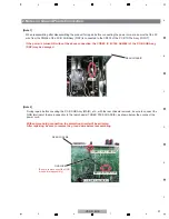
Page 43: ...N206 P C B SUB Assy DSP Connect an alligator clip to the chassis Board to board extension jig cable GGD1630 9 8 Rear chassis Note When reassembling after disassembling the product for repair before connecting the power cord make sure that the 2P wire from the CN206 of the P C B SUB Assy DSP is connected to the CP803 of the P C B TOTAL Assy INPUT See 2 Notes on Ground Points Connection ...

Page 44: ...1FL 1PIN TEST POINT TP201FR 3PIN TEST POINT TP201FR 1PIN TEST POINT TP201C 3PIN TEST POINT TP201C 1PIN TEST POINT TP201SL 3PIN TEST POINT TP201SL 1PIN TEST POINT TP201SR 3PIN TEST POINT TP201SR 1PIN TEST POINT Adjustment Point and Measurement Points see fig1 P C B SUB ASSY AMP fig 1 J SIDE A Idle current VR VR201FL Idle current VR VR201SL Idle current VR VR201C Idle current VR VR201SR Idle current...

Page 45: ...45 VSX 519V K 5 6 7 8 5 6 7 8 A B C D E F ...

Page 46: ...e component parts indicates the importance of the safety factor of the part Therefore when replacing be sure to use parts of identical designation Screws adjacent to b mark on product are used for disassembly For the applying amount of lubricants or glue follow the instructions in this manual In the case of no amount instructions apply as you think it appropriate S E T CORD AC TAPE CLEAR POLY BAG ...

Page 47: ... table 2 NSP 7 Poly Bag 8 PE Sheet 6327040059000 IL 9 Cushion Snow 6230212404000 IL 10 Operating Instructions 5707000001920 IL En Fr Ru NSP 11 Warranty Card ARY7127 NSP 12 Label VRW1629 13 Label Trans 5507000003270 IL NSP 14 Label Getter 519 5507000003610 IL 15 16 Power Cord L068250160020 IL 17 18 NSP 19 Tape 20 Operating Instructions 5707000002100 IL It De NI Es Mark No Description Part No Mark N...

Page 48: ...48 VSX 519V K 1 2 3 4 A B C D E F 1 2 3 4 9 2 EXTERIOR SECTION 1 2 5 3 6 14 8 13 10 11 46 24 12 25 58 1 S9 2 S2 2 S2 C E F CONTACT SIDE NON CONTACT SIDE ...

Page 49: ... 30 31 32 33 34 35 36 37 38 42 18 19 39 41 17 48 49 47 51 40 P I O N E E R 52 25 50 43 44 25 B B 49 S2 25 7 6 S6 34 S3 S4 3 S5 4 2 S2 4 S2 15 S7 10 S2 3 S2 3 S2 5 S2 6 S8 2 S2 2 S2 S1 4 A1 2 S10 Silicon adhesive GYA1011 Silicon grease GEM1057 J D I C N B A M L K P Q 4 5 5 5 A A ...

Page 50: ...R RCA 3Pin JA1001 G606319A1B13Y IL NSP 39 TER Board Screw 4P 40 TER Board Push 4P JA402 G594408SA030Y IL 41 TER Board Push 2P JA102 JA403 G592212A0300Y IL 42 Power Trans 8200960610520 IL 43 Chassis See Contrast table 2 44 Socket Power AC G430000180010 IL 45 Cabinet See Contrast table 2 46 Cushion 4050211205000 IL 47 P C B SUB ASSY H P GUIDE 7028067506010 IL 48 P C B SUB ASSY P T 7028067505010 IL 4...

Page 51: ...B XAM3006 Not used 2 Pioneer Name Plate Not used VAM1129 3 Knob 5080211931100 IL 5087211931000 IL 6 Panel 3067214161100 IL 3067214161200 IL 7 Button 5090213751100 IL 5097213751000 IL 8 Button 5090213761100 IL 5097213761000 IL 9 Button 5097213771100 IL 5097213771000 IL 12 Button 5090213741100 IL 5097213741000 IL 43 Chassis 3207212686110 IL 3207212686100 IL 45 Cabinet 3007211276010 IL 3007211276000 ...

Page 52: ... MAIN and P C B SUB ASSY P T A B P C B SUB ASSY P T 7028067505010 IL B CN701 N CN1001 L CN803 K CP403 M CP402 M CN202 J CP126 A CP125 A CN202 B CN201 B CN1002 L NOTE FOR FUSE REPLACEMENT FOR CONTINUED PROTECTION AGAINST RISK OF FIRE REPLACE WITH SAME TYPE AND RATINGS OF FUSE CAUTION ...

Page 53: ...01 P 1 2 CN202 P 1 2 CN203 P 1 2 Therefore when replacing be sure to use parts of identical designation When ordering service parts be sure to refer to EXPLODED VIEWS and PARTS LIST or PCB PARTS LIST The mark found on some component parts indicates the importance of the safety factor of the part The power supply is shown with the marked box ...

Page 54: ... B C D E F 1 2 3 4 10 2 P C B SUB ASSYS FRONT VOLUME FUNCTION HEADPHONE and PORTABLE C A D E P C B SUB ASSY FRONT 7028067511020 IL C P C B SUB ASSY FUNCTION 7028067514010 IL E P C B SUB ASSY VOLUME 7028067513010 IL D FPC101 A ...

Page 55: ...55 VSX 519V K 5 6 7 8 5 6 7 8 A B C D E F A C F I P C B SUB ASSY HEADPHONE 7028067512010 IL F CP404 M V Video Signal Route Audio Signal Route L ch P C B SUB ASSY PORTABLE 7028067518010 IL I CP802 K ...

Page 56: ...3 4 A B C D E F 1 2 3 4 10 3 P C B SUB ASSY AMP J P C B SUB ASSY AMP 7028067521010 IL J CP801 K FL Audio Signal Route Front L ch FL FL FL SL Audio Signal Route Surround L ch SL SL SL C Audio Signal Route Center ch C C C ...

Page 57: ...57 VSX 519V K 5 6 7 8 5 6 7 8 A B C D E F J CN401 M CP107 A FL FL FL SL SL SL C C C ...

Page 58: ...58 VSX 519V K 1 2 3 4 A B C D E F 1 2 3 4 10 4 P C B SUB ASSY INPUT K P C B SUB ASSY INPUT 7028067531020 IL K CN206 CP118 A P 1 2 ...

Page 59: ...951 Q813 C896 21 23 25 28 CP804 R894 Q812 Q814 J801 12 15 17 19 R804 R815 R934 R935 C834 C836 R952 R953 10 OPTION TABLE C802 C820 SB CH JACK MCACC F AUX AUX Input REMARK SUB WOOFER SIRIUS SB CH F VIDEO NC RCA 610A 00 02 NC NC NC NC NC NC NC 20010WA 03A NC NC NC NC NC VSX 519 NC NC NC NC NC NC NC NC NC NC NC NC NC NC NC 0 K CP120 A CN702 N CN201 J FL Audio Signal Route Front L ch SL Audio Signal Ro...

Page 60: ... H S2 FUNC SW1 L H SW2 COMP_SW1 COMP_MUTE CVBS_S2 CVBS_MUTE TV SAT BD DVD L H COMPONENT DVR VCR LA7956 NJM2586M COMPOSITE INPUT SW L P C B SUB ASSY VIDEO 519 7028067551010 I L CP122 A V Video Signal Route V V V Y Video Signal Route Component Y ch Y Cb Video Signal Route Component Cb ch Cb Cr Video Signal Route Component Cr ch Cr Y Cb Cr ...

Page 61: ...61 VSX 519V K 5 6 7 8 5 6 7 8 A B C D E F L H S1 H L FUNC L H S2 TV SAT BD DVD L H DVR VCR LA7956 COMPOSITE INPUT SW L CP124 A SW Audio Signal Route SubWoofer ch SW ...

Page 62: ...P C B SUB ASSY SPEAKER 519 and P C B SUB ASSY CNT M P C B SUB ASSY SPEAKER 519 7028067601030 IL M CN702 F CN103 A CP203 J CN104 A FL Audio Signal Route Front L ch FL FL FL SL Audio Signal Route Surround L ch SL SL C Audio Signal Route Center ch C C ...

Page 63: ...63 VSX 519V K 5 6 7 8 5 6 7 8 A B C D E F N P C B SUB ASSY CNT 7028067504010 IL N CN702 F CN103 A CP203 J CN104 A CP805 K CP121 A ...

Page 64: ...3 4 A B C D E F 1 2 3 4 10 7 P C B SUB ASSY DSP 1 2 4 2 NO 3 1 R136 CN202 Ref NO IC102 CP105 REMARK NC NC TUC P11X B1 VSX 519 TMS320DA787 P 1 2 P 1 2 P C B SUB ASSY DSP 7028067561020 IL CP114 A CP113 A CP803 K FL SL C SW ...

Page 65: ...X 519V K 5 6 7 8 5 6 7 8 A B C D E F P 1 2 P 2 2 CP114 A CP115 A FL Audio Signal Route Front L ch SL Audio Signal Route Surround L ch C Audio Signal Route Center ch SW Audio Signal Route SubWoofer ch SL C SW ...

Page 66: ...66 VSX 519V K 1 2 3 4 A B C D E F 1 2 3 4 10 8 P C B SUB ASSY DSP 2 2 P 2 2 P 2 2 P C B SUB ASSY DSP 7028067561020 IL P 1 2 CP116 A CP129 A ...

Page 67: ...67 VSX 519V K 5 6 7 8 5 6 7 8 A B C D E F P 2 2 116 ...

Page 68: ...10P CN104 M CP403 CN106 M CP405 CN103 M CP403 CP303 CP301 CP124 AC CORD OR INLET POWER TRANS CP101 POWER TRANS CP102 POWER TRANS CP109 CP107 CN202 CP12 CN201 POWER TRANS IC Q Q125 IC104 IC111 IC112 IC103 IC115 Q122 Q121 Q123 Q124 Q106 Q107 Q108 IC Q Q130 Q129 Q128 Q133 Q127 Q132 Q131 Q126 Q135 Q136 Q134 SIDE A A P C B SUB ASSY MAIN 519 B P C B SUB ASSY P T ...

Page 69: ...19 23P CP112 Q CN1002 CP111 Q CN1001 K CN803 804 806 807 CP117 120 P CN201 204 CP113 116 SIDE A NOTE FOR PCB DIAGRAMS 1 The parts mounted on this PCB include all necessary parts for several destinations For further information for respective destinations be sure to check with the schematic diagram Capacitor Connector P C Board Chip Part SIDE A SIDE B 2 View point of PCB diagrams P T ...

Page 70: ...70 VSX 519V K 1 2 3 4 A B C D E F 1 2 3 4 A B IC108 IC110 IC109 IC120 IC301 IC302 IC106 IC101 IC113 Q300 Q138 Q101 Q111 Q109 Q302 Q110 Q301 Q103 Q202 Q102 Q201 IC Q SIDE B A P C B SUB ASSY MAIN 519 ...

Page 71: ...71 VSX 519V K 5 6 7 8 5 6 7 8 A B C D E F B A SIDE B B P C B SUB ASSY P T ...

Page 72: ...72 VSX 519V K 1 2 3 4 A B C D E F 1 2 3 4 11 2 P C B SUB ASSYS FRONT C R CN802 CP705 E CP703 CN706 POWER TRANS IC Q Q702 Q701 Q703 IC701 IC Q SIDE A SIDE B C P C B SUB ASSY FRONT C P C B SUB ASSY FRONT ...

Page 73: ...73 VSX 519V K 5 6 7 8 5 6 7 8 A B C D E F C A FPC101 VSX 819 23P VSX 519 19P CP704 D CP701 CN704 SIDE A SIDE B ...

Page 74: ...4 11 3 P C B SUB ASSYS VOLUME FUNCTION HEADPHONE and PORTABLE D E F I C CN704 CP701 C CN706 CP703 K CP802 CN705 M CP404 CN702 SIDE A SIDE A D P C B SUB ASSY VOLUME I P C B SUB ASSY PORTABLE F P C B SUB ASSY HEADPHONE E P C B SUB ASSY FUNCTION ...

Page 75: ...75 VSX 519V K 5 6 7 8 5 6 7 8 A B C D E F D E F I IC IC702 Q SIDE B SIDE B I P C B SUB ASSY PORTABLE D P C B SUB ASSY VOLUME F P C B SUB ASSY HEADPHONE E P C B SUB ASSY FUNCTION ...

Page 76: ...VR201SL VR201SR VR201FR VR201FL Q Q205FL Q205SL Q207SL Q207FL Q207SL Q207FL Q207FR Q201FR Q201C Q201FL Q201SR Q205C Q201SL Q205SR Q205FR Q202FR Q206FL Q202FL Q206SL Q206FR Q202SR Q202SL Q203SR Q203FL Q206SR Q204FL Q204FR Q203FR Q204SL Q203SL Q204SR Q204C Q206C Q202C SIDE A SIDE B J P C B SUB ASSY AMP J P C B SUB ASSY AMP ...

Page 77: ...77 VSX 519V K 5 6 7 8 5 6 7 8 A B C D E F J 01 SIDE A SIDE B ...

Page 78: ...2 3 4 11 5 P C B SUB ASSY INPUT K K P CN206 A CP110 G CN701 H CN703 I CN705 CP803 CP804 CP805 CP802 J CN201 CP801 N CN702 CN803 804 806 807 A CP117 120 IC IC803 IC804 IC801 IC802 Q Q816 Q815 Q817 Q818 SIDE A SIDE A K P C B SUB ASSY INPUT ...

Page 79: ...79 VSX 519V K 5 6 7 8 5 6 7 8 A B C D E F K K IC IC801 IC802 Q Q812 Q813 Q814 Q801 Q805 Q804 Q808 Q809 Q810 Q811 Q807 Q806 Q802 Q803 SIDE B SIDE B K P C B SUB ASSY INPUT ...

Page 80: ...80 VSX 519V K 1 2 3 4 A B C D E F 1 2 3 4 11 6 P C B SUB ASSY VIDEO 519 L CN1001 A CP122 CN1002 A CP123 IC Q Q1010 Q1008 IC1001 IC1004 SIDE A L P C B SUB ASSY VIDEO 519 ...

Page 81: ...81 VSX 519V K 5 6 7 8 5 6 7 8 A B C D E F L SIDE A ...

Page 82: ...82 VSX 519V K 1 2 3 4 A B C D E F 1 2 3 4 L IC Q Q1006 IC1003 IC1005 Q1005 Q1002 Q1004 Q1003 Q1001 Q1009 Q1007 Q1011 SIDE B L P C B SUB ASSY VIDEO 519 ...

Page 83: ...83 VSX 519V K 5 6 7 8 5 6 7 8 A B C D E F L SIDE B ...

Page 84: ...84 VSX 519V K 1 2 3 4 A B C D E F 1 2 3 4 11 7 P C B SUB ASSY SPEAKER 519 M M A CN106 CP405 J CP203 CN401 F CN702 CP404 CN104 CP403 A A CN103 CP402 SIDE A SIDE A M P C B SUB ASSY SPEAKER 519 ...

Page 85: ...85 VSX 519V K 5 6 7 8 5 6 7 8 A B C D E F M M IC Q Q404 Q402 Q403 Q401 SIDE B SIDE B M P C B SUB ASSY SPEAKER 519 ...

Page 86: ...9V K 1 2 3 4 A B C D E F 1 2 3 4 11 8 P C B SUB ASSY DSP and P C B SUB ASSY CNT N P K CP803 CN206 A CP113 CN201 A CP114 CN202 A C CN2 CP105 R CN805 IC IC101 IC109 IC110 IC106 IC100 Q SIDE A P P C B SUB ASSY DSP ...

Page 87: ...87 VSX 519V K 5 6 7 8 5 6 7 8 A B C D E F P N A CP115 CN203 A CP116 CN204 UPGRADE CN205 CP200 A CP129 A CP121 CN701 K CP805 CN702 SIDE A N P C B SUB ASSY CNT ...

Page 88: ...88 VSX 519V K 1 2 3 4 A B C D E F 1 2 3 4 N P IC Q Q802 IC806 SIDE B P P C B SUB ASSY DSP N P C B SUB ASSY CNT ...

Page 89: ...89 VSX 519V K 5 6 7 8 5 6 7 8 A B C D E F P N SIDE B ...

Page 90: ...90 VSX 519V K 1 2 3 4 A B C D E F 1 2 3 4 11 9 P C B SUB ASSY HDMI 519 Q Q A CP111 CN1001 A CP112 CN1002 IC IC1001 IC1002 IC1003 Q SIDE A SIDE A Q P C B SUB ASSY HDMI 519 ...

Page 91: ...91 VSX 519V K 5 6 7 8 5 6 7 8 A B C D E F Q Q IC IC1005 Q Q1002 Q1004 Q1001 Q1003 Q1201 Q1405 Q1402 Q1403 Q1401 Q1204 SIDE B SIDE B Q P C B SUB ASSY HDMI 519 ...

Page 92: ...2 P C B SUB ASSY INPUT 7028067531020 IL NSP 1 P C B TOTAL ASSY VIDEO 519 7025HK0812014 IL 2 P C B SUB ASSY VIDEO 519 7028067551010 IL NSP 1 P C B TOTAL ASSY DSP 7025HK0812015 IL 2 P C B SUB ASSY DSP 7028067561020 IL NSP 1 P C B TOTAL ASSY HDMI 519 7025HK0812016 IL 2 P C B SUB ASSY HDMI 519 7028067581010 IL NSP 1 P C B TOTAL ASSY MAIN 7025HK0812010 IL 2 P C B SUB ASSY MAIN 7028067501020 IL 2 P C B ...

Page 93: ...ENCODER G121123040010 IL Mark No Description Part No E P C B SUB ASSY FUNCTION SEMICONDUCTORS D 711 712 K005041480030 IL MISCELLANEOUS S 701 SW ENCODER G121123050020 IL S 715 SWITCH G180040500010 IL F P C B SUB ASSY HEADPHONE SEMICONDUCTORS D 705 706 K005041480030 IL MISCELLANEOUS JA 701 JACK D6 5 G402PJ619AG0Y IL I P C B SUB ASSY PORTABLE SEMICONDUCTORS D 713 714 K005041480030 IL MISCELLANEOUS JA...

Page 94: ...017 R401L R401R C060033166520 IL CAPACITORS C 4013 4017 D02010306C060 IL C 4022 4024 4026 4027 D02047306C060 IL Mark No Description Part No N P C B SUB ASSY CNT P C B SUB ASSY CNT has no service part P P C B SUB ASSY DSP SEMICONDUCTORS IC 100 J001421640040 IL IC 101 J005291600040 IL IC 102 J080320788010 IL IC 103 REG103 J126111700041 IL IC 106 J040742570030 IL IC 109 J080458800010 IL IC 110 J04074...

Reviews: