27
VSX-519V-K
5
6
7
8
5
6
7
8
A
B
C
D
E
F
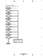
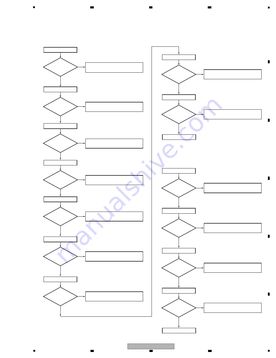
To Step 5
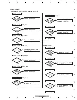
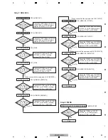
Step 4: X'TAL
Replace IC1003 or X1401.
Replace IC1001 or X1001.
Is there
a 12 MHz
output?
Is there
a 12 MHz
output?
Is there
a 27 MHz
output?
Is there
a 27 MHz
output?
IC1003 (Pin 15)
No
Yes
IC1003 (Pin 13)
No
Yes
Check the path to pin13 of IC1003.
Replace IC1003.
IC1001 (Pin 5)
No
Yes
IC1001 (Pin 4)
No
Yes
Check the path to pin4 of IC1001.
Replace IC1001.
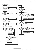
To Step 4
Check the parts and patterns in
the path pin 87 of IC1003.
Is the voltage
0 to 3.3 V?
Is there a data
0 to 3.3 V?
IC1001 (Pin 21)
No
HR_RST
Yes
IC1002 (Pin 25)
No
Yes
Check the parts and patterns in
the path pin 89 of IC1003.
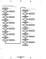
Step 3: Diagnosis
CN1002 (Pin 6)
Is the voltage
0 to 3.3 V?
No
CE
Diagnose the MAIN Assy.
Diagnose the MAIN Assy.
Diagnose the MAIN Assy.
Diagnose the MAIN Assy.
Diagnose the MAIN Assy.
Yes
CN1002 (Pin 7)
Is the voltage
0 to 3.3 V?
No
SUB_PDN
CN1002 (Pin 3)
Is there
a data input?
(0 to 3.3 V)
Is there
a data input?
(0 to 3.3 V)
No
CSCK_MAIN
Yes
Yes
CN1002 (Pin 8)
Is there
a data input?
(0 to 3.3 V)
No
MAIN_IRQ
Yes
CN1002 (Pin 9)
Is there
a data output?
(0 to 3.3 V)
Is there
a data output?
(0 to 3.3 V)
No
SUB_IRQ
Check the parts and patterns in
the path IC1003.
Yes
CN1002 (Pin 4)
No
SCDO_MAIN
Yes
CN1002 (Pin 5)
No
SCDI_MAIN
Yes
Check the parts and patterns in
the path IC1003.
Each data lines confirmation checks it after standby OFF/ON.
Summary of Contents for VSX-519V-K
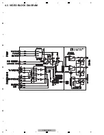
Page 18: ...18 VSX 519V K 1 2 3 4 A B C D E F 1 2 3 4 4 3 VIDEO BLOCK DIAGRAM P C B SUB ASSY VIDEO 519 L ...
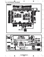
Page 19: ...19 VSX 519V K 5 6 7 8 5 6 7 8 A B C D E F 4 4 U COM BLOCK DIAGRAM P C B SUB ASSY FRONT C ...
Page 45: ...45 VSX 519V K 5 6 7 8 5 6 7 8 A B C D E F ...
Page 57: ...57 VSX 519V K 5 6 7 8 5 6 7 8 A B C D E F J CN401 M CP107 A FL FL FL SL SL SL C C C ...
Page 67: ...67 VSX 519V K 5 6 7 8 5 6 7 8 A B C D E F P 2 2 116 ...
Page 71: ...71 VSX 519V K 5 6 7 8 5 6 7 8 A B C D E F B A SIDE B B P C B SUB ASSY P T ...
Page 77: ...77 VSX 519V K 5 6 7 8 5 6 7 8 A B C D E F J 01 SIDE A SIDE B ...
Page 81: ...81 VSX 519V K 5 6 7 8 5 6 7 8 A B C D E F L SIDE A ...
Page 83: ...83 VSX 519V K 5 6 7 8 5 6 7 8 A B C D E F L SIDE B ...
Page 89: ...89 VSX 519V K 5 6 7 8 5 6 7 8 A B C D E F P N SIDE B ...


