35
VSX-519V-K
5
6
7
8
5
6
7
8
A
B
C
D
E
F
[3] The unit’s operation when a error is detected
[Purpose]
[Basic operations]
FL Display
Description of Indications
Key Operation
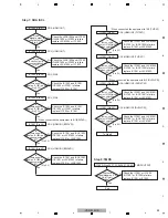
3.1 DC (AMP is abnormality) error detection
(Normal display)
(DC detection)
(Auto)
(RECEIVER POWER OFF)
usually
*1, *2
Normal display
Time (sec.)
• The unit’s operation when a DC/OVER/TEMP error is detected is described here.
• How to cancel the status after detection of a DC error is described here, because no key input will be
accepted after a DC error detection.
*1 The time required for the unit to be shut off after an error is detected depends on the circuit configuration.
*2 If the unit is automatically shut off after a DC error is detected, no key input will be accepted afterward.
(The power will not be turned ON.)
To turn it on again, see “3.4 How to cancel the status after detection of a DC error” below.
A key input will not be inhibited after an OVERLOAD/TEMP error is detected. (The unit can be turned ON.)
Simultaneously holding the [ADVANCD SURROUND] and [STANDBY/ON] keys on the
front panel pressed for 2 seconds will cancel Key Input Inhibition mode after a DC error
detection and turn the unit ON.
[Detailed explanations]
FL Display
Description of Indications
Key Operation
3.2 OVERLOAD (overcurrent) error detection
(Normal display)
(OVERLOAD detection)
(Auto)
(RECEIVER POWER OFF)
usually
*1
Normal display
Time (sec.)
FL Display
Description of Indications
Key Operation
3.3 TEMP (AMP overheat) error detection
(Normal display)
(TEMP detection)
(Auto)
(RECEIVER POWER OFF)
usually
*1
Normal display
Time (sec.)
FL Display
Description of Indications
Key Operation
3.4 How to cancel the status after detection of the DC error
(STANDBY state)
(Normal display)
usually
Normal display
Time (sec.)
[ADVANCED SURROUND]
+ [STANDBY/ON]
(press and hold the keys
for 2 seconds.)
Summary of Contents for VSX-519V-K
Page 18: ...18 VSX 519V K 1 2 3 4 A B C D E F 1 2 3 4 4 3 VIDEO BLOCK DIAGRAM P C B SUB ASSY VIDEO 519 L ...
Page 19: ...19 VSX 519V K 5 6 7 8 5 6 7 8 A B C D E F 4 4 U COM BLOCK DIAGRAM P C B SUB ASSY FRONT C ...
Page 45: ...45 VSX 519V K 5 6 7 8 5 6 7 8 A B C D E F ...
Page 57: ...57 VSX 519V K 5 6 7 8 5 6 7 8 A B C D E F J CN401 M CP107 A FL FL FL SL SL SL C C C ...
Page 67: ...67 VSX 519V K 5 6 7 8 5 6 7 8 A B C D E F P 2 2 116 ...
Page 71: ...71 VSX 519V K 5 6 7 8 5 6 7 8 A B C D E F B A SIDE B B P C B SUB ASSY P T ...
Page 77: ...77 VSX 519V K 5 6 7 8 5 6 7 8 A B C D E F J 01 SIDE A SIDE B ...
Page 81: ...81 VSX 519V K 5 6 7 8 5 6 7 8 A B C D E F L SIDE A ...
Page 83: ...83 VSX 519V K 5 6 7 8 5 6 7 8 A B C D E F L SIDE B ...
Page 89: ...89 VSX 519V K 5 6 7 8 5 6 7 8 A B C D E F P N SIDE B ...


