32
VSX-819H-K
1
2
3
4
A
B
C
D
E
F
1
2
3
4
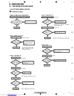
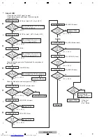
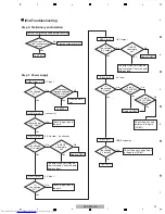
Step 2: Operation of USB Media control IC
Is there
a 12 MHz
output?
USB_RX and USB_TX should
be high during operation.
Check the pattern in the path.
FRO
N
T Assy and MAI
N
Assy
Check the parts and patterns in the path.
Replace XTAL1, etc.
Yes
N
o
Yes
N
o
IC
8
01 (pins 54,55)
C
N8
02 USB_RX, TX (Pins 4, 5)
IC
8
01 (pin 44) -> IC
8
03 (pin 3
8
)
XI
N
/XOUT
Do
USB_RX and USB_TX
communication with
main micom?
Operation of IC
8
01 is OK.
To STEP 3
Operation of IC
8
01 is OK.
To STEP 3
DATA and ADDRESS lines
between SDRAM (IC
8
03),
FLASH ROM (IC
8
02) and IC
8
01
are may not be connected.
D+ and D- should have
waveform during normal
condition.
Check the pattern in the path.
IC
8
01, etc.
Are
there the waveforms
like figure?
After
turning the power
on and several seconds
later, does SDCLK change
12 MHz to
8
0 MHz?
Yes
Yes
N
o
N
o
C
N8
01 (pins 2,3)
D+/D-
Initial communication [SDCLK]
Fig. D+
X: 1
μ
S/div, Y: 2
V
/div
X: 1
μ
S/div, Y: 2
V
/div
Fig. D-
Yes
Is
C
N8
02 pins 1, 2, 3
(RESET, RDY, PD
N
)
high?
Yes
Check
C
N
705, C
N
704 of
FRO
N
T and MAI
N
Assy.
N
o
N
o
Check the path to
MAI
N
Assy.
Summary of Contents for VSX-819H-K - AV Receiver - Gloss
Page 19: ...19 VSX 819H K 5 6 7 8 5 6 7 8 A B C D E F 4 4 U COM BLOCK DIAGRAM P C B SUB ASSY FRONT C ...
Page 49: ...49 VSX 819H K 5 6 7 8 5 6 7 8 A B C D E F ...
Page 55: ...55 VSX 819H K 5 6 7 8 5 6 7 8 A B C D E F ...
Page 61: ...61 VSX 819H K 5 6 7 8 5 6 7 8 A B C D E F J CN401 M CP107 A FL FL FL SL SL SL C C C ...
Page 71: ...71 VSX 819H K 5 6 7 8 5 6 7 8 A B C D E F P 2 2 CN805 R 116 ...
Page 73: ...73 VSX 819H K 5 6 7 8 5 6 7 8 A B C D E F R CP105 A CP705 C ...
Page 77: ...77 VSX 819H K 5 6 7 8 5 6 7 8 A B C D E F B A SIDE B B P C B SUB ASSY P T ...
Page 83: ...83 VSX 819H K 5 6 7 8 5 6 7 8 A B C D E F J 01 SIDE A SIDE B ...
Page 87: ...87 VSX 819H K 5 6 7 8 5 6 7 8 A B C D E F L SIDE A ...
Page 89: ...89 VSX 819H K 5 6 7 8 5 6 7 8 A B C D E F L SIDE B ...
Page 95: ...95 VSX 819H K 5 6 7 8 5 6 7 8 A B C D E F P N SIDE B ...

