background image


EL640.200-SK Operations Manual (020-0348-00B) 

10 

Video Input Signals 

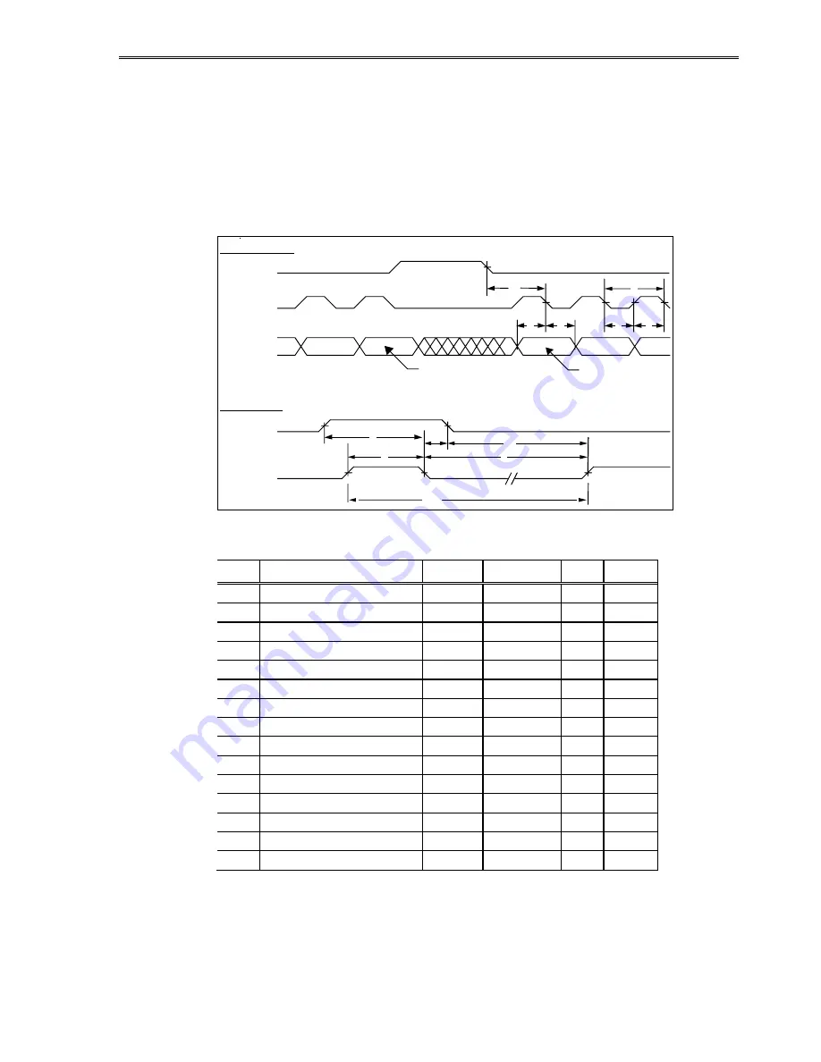
The end of the top line of a frame is marked by VS, vertical sync signal as 
shown in Figure . The end of each row of data is marked by HS. In non-buffered 
mode, the VS signal may be independently set to a CMOS low level at any time 
for longer than one frame period. During the time of VS inactivity the display is 
blank. Halting VS results in a standby condition to minimize power usage in 
buffered mode.  
 

HS

VCLK

VID0-3

VS

HS

3

First Line VID

4

1

Pixels:  w x y z

Horizontal Timing


Vertical Timing


Pixels:  a b c d

5

6

9

10

7

11

8

2

Second Line VID Data

12


Figure 3. Video Input Timing Diagram. 

Table 5. Video Input Descriptions. 

Num  Description 

Symbol 

Min. 

Max. 

Units 

HS high time  

tHSh 

125 


nsec 

HS low time 

tHSl 

160 


tVCLK 

HS to VCLK  

tHSsu 

63 


nsec 

VID setup to VCLK 

tVIDsu 

100 


nsec 

VID hold from VCLK 

tVIDhd 

100 


nsec 

Video clock period 

tVCLK 

334 (200*) 


nsec 


VCLK rise, fall time 

tVCLKrf 


50 

nsec 

VCLK low width 

tVCLKl 

125 


nsec 

VCLK high width 

tVCLKh 

125 


nsec 

VS high setup to HS low 

tVShsu 

100 


nsec 

10 

VS hold after HS 

tVShd 

100 


nsec 

11 

VS low setup to HS high 

tVSlsu 

140 


nsec 

12 

HS period 

tHS 

 53.6 (41.3*) 


µsec 


VS period 

tVS 

200 (101*) 


tHS 


Max frame rate* 


239* 


Hz 

* Non-buffered mode 

Summary of Contents for ICEBrite EL640.200-SK ALE

Page 1: ...EL640 200 SK ICEBrite Half VGA Display USER S MANUAL www planar com...

Page 2: ...Revision Control Date Description July 2000 Document number OM250 01 June 2004 Document number 020 0348 00A June 2005 Document number 020 0348 00B...

Page 3: ...face Information 9 Buffered Video Mode 9 Non buffered Video Mode 9 Video Input Signals 10 Video Data in Non Buffered Mode 11 Video Data in Buffered Mode 11 Dimming 12 Analog Luminance Control 12 Self...

Page 4: ...ce of Data in Buffered Mode 11 Figure 6 Display Dimensions 16 Tables Table 1 DC Input Voltage Requirements 6 Table 2 Video Input Requirements 6 Table 3 Power Consumption 7 Table 4 Connector Pinouts 8...

Page 5: ...eliminating the blooming common to other high bright displays The display consists of an EL glass panel and control electronics assembled into a space saving rugged package for easy mounting The EL64...

Page 6: ...support failure to do so will bend the display and cause the glass to break The instrument enclosure or frame should not flex or distort in such a way that during use the bending loads might be transf...

Page 7: ...leaning cloths are recommended to minimize the risk of inadvertently scratching the display with particles embedded in a re used cloth Particular care should be taken when cleaning displays with anti...

Page 8: ...Symbol Min Typ Max Absolute Max 2 Logic voltage VL 4 75 V 5 25 V Logic voltage absolute max VLmax 0 5 V 6 V Logic supply current at 5 V IL 150 mA Display supply voltage VH 8 V 18 V 20 V VH Supply curr...

Page 9: ...7 8 1 10 4 Absolute Maximum estimated W 70 of pixels on per row 4 5 9 13 17 Typical W 20 of pixels on per row 3 0 4 7 6 2 7 5 Figure 1 EL640 200 SK Power Curve typical 100 luminance level 0 00 2 00 4...

Page 10: ...Power Connector Table 4 Connector Pinouts Pin Signal Description Pin Signal Description 1 VID1 U1 Video Data 2 VID0 U0 Video Data 3 VID3 U3 Video Data 4 VID2 U2 Video Data 5 VID L3 Video Lower Panel 6...

Page 11: ...ion is available see Dimming on page 11 Due to the timing independence of the input data and the display scan an image will be shown on the display even without any video input data When using averagi...

Page 12: ...z Horizontal Timing Vertical Timing Pixels a b c d 5 6 9 10 7 11 8 2 Second Line VID Data 12 Figure 3 Video Input Timing Diagram Table 5 Video Input Descriptions Num Description Symbol Min Max Units...

Page 13: ...0 U1 1 160 U1 100 160 L1 1 160 L1 100 160 U2 1 160 U2 100 160 L2 1 160 L2 100 160 Column 1 Column 640 Row 100 Row 101 Figure 4 Pixel Location versus Sequence of Data in Non buffered Mode Video Data in...

Page 14: ...ble 6 Digital Luminance Control Approx Relative Luminance Max 75 50 25 LUM1 1 1 0 0 LUM0 1 0 1 0 Frame rate Hz 240 180 120 60 Analog Luminance Control Luminance control circuitry is provided to allow...

Page 15: ...is pulled high during normal operation the display will enter the self test mode Optical Table 8 Optical Characteristics Luminance Lon areal min Lon areal typ Loff areal max 63 5 cd m 80 6 cd m 20 cd...

Page 16: ...5 C per IEC 68 2 30 Altitude Operating non operating 0 to 18 km 58k ft per IEC 68 2 13 Vibration operating non operating Random 0 02 g 2 Hz 5 500 Hz 30 minutes each axis per IEC 68 2 34 operating non...

Page 17: ...10 79 oz Fill Factor 59 3 Display Active Area millimeters inches width 211 17 8 31 height 79 17 3 12 diagonal 225 52 8 87 Pixel Size millimeters inches width 25 0 009 height 31 0 012 Component Envelo...

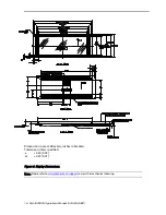
Page 18: ...ual 020 0348 00B 16 Dimensions in are millimeters inches in brackets Tolerances unless specified x r0 50 0 02 xx r0 25 0 01 Figure 6 Display Dimensions Note Please refer to www planar com support to v...

Page 19: ...insufficient Seller shall refund Buyer s paid price for the Goods and have no other liability to Buyer All warranty repairs must be performed at Seller s authorized service center using parts approved...

Page 20: ...pport and service are available to make the integration of Planar displays as simple and quick as possible for our customers RMA Procedure For a Returned Material Authorization number please contact P...

Page 21: ...ope and Asia Pacific Support Olarinluoma 9 P O Box 46 FIN 02201 Espoo Finland Tel 358 9 420 01 Hours M F 7 00am 4pm CET 2005 Planar Systems Inc 06 05 Planar is a registered trademark of Planar Systems...

Reviews: