LC640.480.21-065 Operations Manual (OM610-00)
9
Power Sequencing (LCD)
When performing power sequencing:
•
Ensure the supply voltage for input signals is the same as for VCC.
•
Apply VCC within the LCD operation period. When the backlight turns on before
LCD operation or the LCD operation turns off before the backlight turns off, the
display may momentarily become white.
•
When the power is off, keep whole signals (Hsync, Vsync, CLK, DE, and DATA)
low level or high impedance.
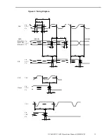
Figure 3. Power Sequencing.
SUPPLY VOLTAGE SEQUENCE
VCC
Signal
VALID
Power-on
Power-off
4.75 V
4.75 V
0 V
0 V
0 <t<35 ms
0 <t<35 ms
ms
t<150
*
1
The supply voltage for input signals should be the same as VCC.
*2
Apply VDD within the LCD operation period. When the backlight turns on before LCD operation or the LCD
operation turns off before the backlight turns off, the display may momentarily become white.
*3
When the power is off, please keep whole signals (Hsync, Vsync, CLK, DE, and DATA) low level or high
impedance.
Video Signals
Video Signal Characteristics
Video signal inputs on J1 are digital inputs and are compatible with CMOS logic.
Table 7. Video Signal DC Characteristics.
Description
Symbol
Minimum
Maximum
Units
Absolute maximum input voltage
V
I
max
-0.3
6.5
Vdc
Low-level input voltage
V
IL
0
0.8
Vdc
High-level input voltage
V
IH
2.2
5.25
Vdc


