COM Express
™
PORTWELL PCOM-B634VG User's Guide
Copyright © PORTWELL 2015 PCOM-B634VG User's Guide
31
5 Signal Descriptions and Pin out Tables
Signal Tables Terminology Descriptions
I
Input to the Module
O
Output from the Module
I/O
Bi-direction input / output signal
OD
Open Drain output
CMOS
Logic input or output. Input thresholds and output levels shall be 80% of supply rail for high side and 20% of the
relevant supply rail for low side.
PCIE
PCI Express compatible differential signal. Please refer to the PCI Express Specification for details. PCIE transmit
pins (Module outputs) shall be AC coupled on the Module. PCIE receive pins (Module inputs) shall be DC coupled
on the COM Express® Module and shall be assumed to be AC coupled off Module, close to the signal source. If the
target PCI Express device resides on the Carrier Board, the Module PCIE receive lanes (target PCIE device
transmit lanes) shall be AC coupled near the device on the Carrier Board. If the Carrier Board implements a PCIE
slot, then these signals shall be AC coupled on the add-in card, not on the Carrier Board.
SATA
SATA compatible differential signal. Please refer to the SATA Specification for details. All COM Express® SATA
signals shall be AC coupled on the Module.
LVDS
Low Voltage Differential Signal – 330mV nominal; 450mV maximum differential signal.
Analog
Inputs and Outputs used for LAN, and VGA are analog signals.
PU
Pull-up resistor on PCOM-B634VG
PD
Pull-down resistor on PCOM-B634VG
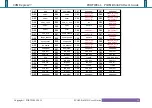
Table 10 Signal Tables Terminology Descriptions
<Caution>
10GbE pin definition is not defined in COM Express specification rev2.0, below 10GbE pin out is defined by Portwell itself. Please contact Portwell
for more information while designing your own carrier.

