Important
note
Service Manual
PCB Replacement Procedures
7 - 31
3x3 UPS
Issue 2 - November 2001
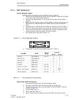
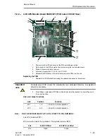
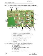
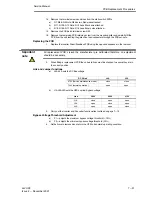
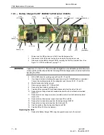
14. Remove the terminal screws and wires from the static switch SCRs.
a)
N7, N8 & N9 Note: N8 has two Red wires attached.
b)
N11, N12 & N13 Note: N12 has a Black wire attached.
c)
N15, N16 & N17 Note: N16 has a Brown wire attached.
15. Remove the PCB Earth terminal screw N20.
16. Remove the remaining PCB retaining screw from the mounting pillar and carefully lift the
PCB from the unit feeding the gate drive lead connectors through the PCB cutĆouts.
Replacing the PCB
1.
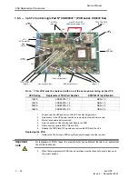
Replace the Inverter Driver/Feedback PCB using the opposite sequence to the removal.
All replacement PCB's leave the manufacturer pre calibrated therefore no adjustment
should be necessary.
2.
When fitting a replacement PCB the on board links must be checked to ensure they are in
the correct position.
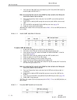
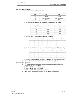
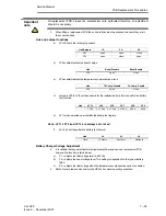
Link and Jumper functions
a)
J4AĆJ5A sets the DC Bus voltage.
DC V/Link
J4A
J5A
375V (
s
ervice maintenance mode)
close
close
750V (normal operation.)
open
open
b)
JIAĆJ2AĆJ3A sets the UPS nominal bypass voltage;
Link
380V
400V
415V
J1A
close
open
open
J2A
open
close
open
J3A
open
open
close
3.
Carry out the Inverter and Converter functional test outlined on page 7-15.
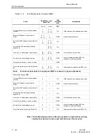
Bypass Voltage Threshold Adjustment
a)
P1 = adjusts the maximum bypass voltage threshold (+10%)
b)
P2 = adjusts the minimum bypass voltage threshold (Ć10%)
4.
Refit all covers removed and return the UPS to its normal operating condition.

