Service Manual
PCB Replacement Procedures
7 - 34
3x3 UPS
Issue 2 - November 2001
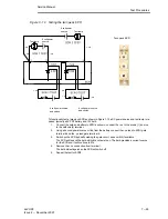
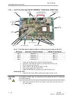
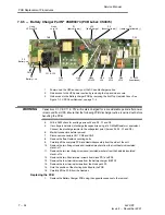
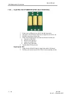
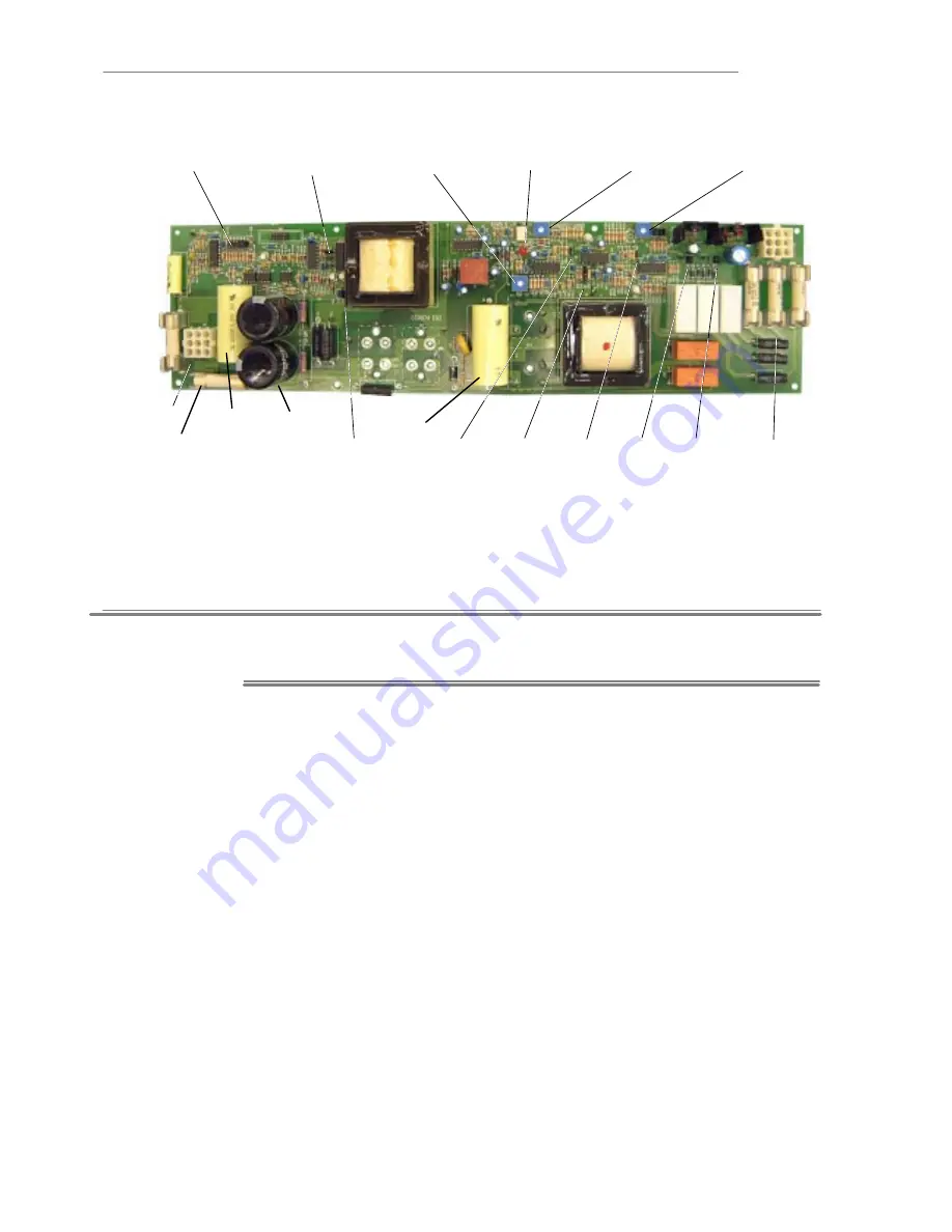
7.9.5 - Battery Charger Part Nº 0SDE0074 (PCB Label: CS0074)
LD1
(float Charge)
CN1
Links
JP5 to JP10
CN2
CN3
P1
(float volts adj.)
P2
(boost volts adj.)
P3
(temp. comp float adj.)
Links
J4 to J5
Link
JP11
F1 F2 F3
(Input fuses)
F5
Battery ćve
Links
JP1 JP2
Link
JP12
Link
JP13
Link
JP3
Link
JP4
C9
F4
ve
C1
C11 & C12
1.
Power down the UPS and carry out the DC bus discharge routine.
2.
Gain access to the UPS power section by removing the top and side covers.
3.
Gain access to the Battery charger PCB by removing the front Top Heatsink Cover. See
Figure 7-1 UPS Cover Removal on page 7-3.
WARNING
Capacitors C1, C9, C11 & C12 will remain charged for a considerable period after power
is removed from UPS. Ensure that the following PCB discharge routine is carried out before
handling the PCB.
4.
With a DVM check for a voltage across F4 and F5, C1 and C9.
5.
If a voltage is detected, discharge the capacitors using a 1k
Ù
4Watt Resistor or equivalent.
Connect the discharge resistor to the voltage test point. (Across F4, F5, C1 and C9).
6.
Mark all connectors before removal.
7.
Disconnect connectors CN1, CN2 and CN3.
8.
Remove the ftwo Heatsink securing bolts.
9.
Carefully lift the complete PCB and Heatsink assembly from the side of the unit.
10. Remove the two fixing screws and insulated washers from the front heatsink insulated
stand-off.
11. Remove the two rear fixing screws and insulated washers from the heatsink insulated
stand-off's.
12. Remove the two Allen terminal screws from diods PD1 and PD2.
13. Remove the four terminal screws from the battery charger IGBT Q1.
14. Remove the four terminal screws from the diode pack D1.
15. Note the position of the shorting links fitted to the PCB.
16. Carefully lift the PCB from the Heatsink.
Replacing the PCB
1.
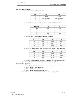
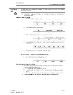
Replace the Battery Charger PCB using the opposite sequence to the removal.

