85
Prestigio Cavaliere 141
Technical Service Manual
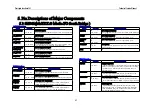
5. Pin Descriptions of Major Components
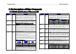
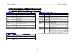
P C I In ter fa ce
Na m e
P in Attr
Sign a l Descr ip tion
AD[31:0]
I/O
3.3V/5V -M
P C I Ad d r ess /Da ta Bu s:
In address phase:
1.When the SiS961 is a PCI bus master, AD[31:0] are output
signals.
2.When the SiS961 is a PCI target, AD[31:0] are input signals.
In data phase:
1.When the SiS961 is a target of a memory read/write cycle,
AD[31:0] are floating.
2.When the SiS961 is a target of a configuration or an I/O cycle,
AD[31:0] are output signals in a read cycle, and input signals in
a write cycle.
P AR
I/O
3.3V/5V -M
P a r ity:
SiS961 drives out Even Parity covering AD[31:0] and
C/BE[3:0]#. It does not check the input parity signal.
F R AM E #
I/O
3.3V/5V -M
F r a m e#:
FRAME# is an output when the SiS961 is a PCI bus master.
The SiS961 drives FRAME# to indicate the beginning and
duration of an access. When the SiS961 is a PCI slave device,
FRAME# is an input signal.
IR DY#
I/O
3.3V/5V -M
In itia tor R ea d y:
IRDY# is an output when the SiS961 is a PCI bus master. The
assertion of IRDY# indicates the current PCI bus master's
ability to complete the current data phase of the transaction. For
a read cycle, IRDY# indicates that the PCI bus master is
prepared to accept the read data on the following rising edge of
the PCI clock. For a write cycle, IRDY# indicates that the bus
master has driven valid data on the PCI bus. When the SiS961 is
a PCI slave, IRDY# is an input pin.
T R DY#
I/O
3.3V/5V -M
T a r get R ea d y:
TRDY# is an output when the SiS961 is a PCI slave. The
assertion of TRDY# indicates the target agent's ability to
complete the current data phase of the transaction. For a read
cycle, TRDY# indicates that the target has driven valid data
onto the PCI bus. For a write cycle, TRDY# indicates that the
target is prepared to accept data from the PCI bus. When the
SiS961 is a PCI master, it is an input pin.
ST O P #
I/O
3.3V/5V -M
Stop #:
STOP# indicates that the bus master must start terminating its
current PCI bus cycle at the next clock edge and release control
of the PCI bus. STOP# is used for disconnection, retry, and
target-abortion sequences on the PCI bus.
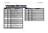
P C I In ter fa ce C on tin u e
Na m e
P in Attr
Sign a l Descr ip tion
DE VSE L #
I/O
3.3V/5V -M
Device Select:
As a PCI target, SiS961 asserts DEVSEL# by doing positive or
subtractive decoding. SiS961 positively asserts DEVSEL# when
the DRAM address is being accessed by a PCI master, PCI
configuration registers or embedded controllers’ registers are
being addressed, or the BIOS memory space is being accessed.
The low 16K I/O space and low 16M memory space are
responded subtractively. The DEVESEL# is an input pin when
SiS961 is acting as a PCI master. It is asserted by the addressed
agent to claim the current transaction.
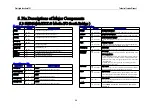
P R E Q [4:0]#
I
3.3V/5V -M
P C I Bu s R eq uest:
PCI Bus Master Request Signals
P G NT [4:0]#
O
3.3V –M
P C I Bu s G r a nt:
PCI Bus Master Grant Signals
P R E Q 5# /
G P IO 5
I
I/O
3.3V/5V- M
P C I Bu s R eq uest:
PCI Bus Master Request Signal
P G NT 5# /
G P IO 6
O
I/O
3.3V- M
P C I Bu s G r a nt:
PCI Bus Master Grant Signal
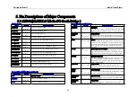
INT [A:D]#
I
3.3V/5V –M
P C I in ter r u p t A,B,C ,D:
The PCI interrupts will be connected to the inputs of the internal
Interrupt controller through the rerouting logic associated with
each PCI interrupt.
P C IR ST #
O
3.3V –M
P C I Bu s R eset:
PCIRST# will be asserted during the period when PWROK is
low, and will be kept on asserting until about 24ms after
PWROK goes high.
SE R R #
I
3.3V/5V –M
System E r r or :
When sampled active low, a non-maskable interrupt (NMI) can
be generated to CPU if enabled.
5.3 SiS961(MuTIOL® Media I/O South Bridge )

