V6402, V6404, V6406, V6408
and V6418 HD converters
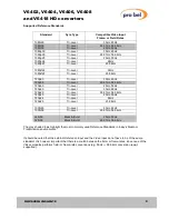
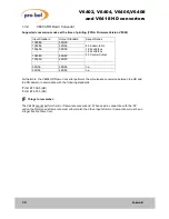
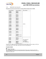
HU-V6402&4&6&8&18
21
Notes:
1. In this case, a pixel is a luminance sample.
2. When in Short Delay Down Conversion mode, these conversions have a maximum insertion delay of 1
ms.
2.6
Hardware
2.6.1
The PCB
This figure shows the construction of the PCB, along with some components of interest. Note that the
main I/O connector is in fact mounted on a daughter board, which is held down by two screws. The Down
and Cross Converters also have a large sub-board mounted on the centre of the board.
The main connector is a 220-way 2mm press-fit connector. When new there may be a substantial
insertion force when mating with a rear module; this is normal. However, it is important that the module is
not plugged into one of Vistek’s conventional units with significant force. If so then it is possible to break
off one of the locating lugs.
2.6.2
Links and Switches
The purposes of the links and switches are shown in the following table. Details of their operation are
described in later sections.
ITEM
Title
Comments
SW1
RESET
Used to reset the internal microcontroller.
JP1
Debug
For development and test use only. (May not be
fitted)
JP2
H8 Program
For development and test use only. (May not be
fitted)
PL1
JTAG Port
Never used in operation. (May not be fitted)
JP3
JTAG Enable
For Test. Fit in 2-3 position.
SW
Video REF Term
Slider up
– Terminated with 75
Ω
Slider down
– Hi-Z (un-terminated)
PL1
JP3
JP2
JP1
S
W1
Flash Memory Card
F
ron
t
P
anel
I/O
D
au
gh
ter
Boa
rd
R
e
a
r
C
o
nne
c
tor
FS1
SW
Video
P
roc
es
sing
D
aug
hte
r B
oa
rd
(V
64
04
, V
640
6, V
640
8, V
64
18)


