background image

Appendix  C  Trouble Shooting

PC-550 USER

S MANUAL

Page: C-3

DISKETTE DRIVES OR TYPES MISMATCH ERROR :

When the diskette drive type is different from CMOS, please run setup or
configure the drive again.

ERROR ENCOUNTERED INITIALIZING HARD DRIVE :

When you can‘t initialize the hard drive. Assure the adapter is installed
correctly and all cables are correctly and firmly attached. Also be sure the
correct hard drive type is selected in Setup.

ERROR INITIALIZING HARD DISK CONTROLLER :

When this error occurs. Be sure the cord is exactly installed in the bus.
Make sure the correct hard drive type is selected in Setup. Also check
whether all of the jumpers are set correctly in the hard drive.

FLOPPY DISK CONTROLLER ERROR OR
NO CONTROLLER PRESENT :

When you cannot find or initialize the floppy drive controller, please check
the controller whether in proper Setup. If there are no floppy drive installed,
Ensure the Diskette Drive selection in Setup is set to NONE.

KEYBOARD ERROR OR NO KEYBOARD PRESENT 

:

When this situation happens, please check keyboard attachment and no keys
being pressed during the boot. If you are purposely configuring the system
without a keyboard, set the error halt condition in Setup to HALT ON ALL,
BUT KEYBOARD. This will cause the BIOS to ignore the missing
keyboard and continue the boot.

MEMORY ADDRESS ERROR :

When the memory address indicates error. You can use this location along
with the memory map for your system to find and replace the bad memory
chips.

MEMORY SIZE HAS CHANGED :

Memory has been added or removed since the last boot. In EISA mode, use
Configuration Utility to reconfigure the memory configuration. In ISA mode
enter Setup and enter the new memory size in the memory fields.

Summary of Contents for ProX-1550

Page 1: ...USER S MANUAL ...

Page 2: ... in installing and setting up the system The infor mation contained in this document is subject to change without any notice This manual is copyrighted March 2000 You may not reproduce or transmit in any form or by any means electronic or mechanical including photocopying and recording ACKNOWLEDGEMENTS All trademarks and registered trademarks mentioned herein are the property of their respective o...

Page 3: ... 2 11 2 4 7 AMD K6 200 233 CPU Type Clock Jumper Settings 2 12 2 4 8 AMD K6 2 266 300 CPU Type Clock Jumper Settings 2 13 2 4 9 AMD K6 2 333 350 CPU Type Clock Jumper Settings 2 14 2 4 10 AMD K6 2 366 380 CPU Type Clock Jumper Settings 2 15 2 4 11 AMD K6 2 400 450 CPU Type Clock Jumper Settings 2 16 2 4 12 AMD K6 2 450 500 CPU Type Clock Jumper Settings 2 17 2 4 13 AMD K6 3 400 450 CPU Type Clock ...

Page 4: ...Connector 2 33 2 28 SCSI Connector 2 34 2 29 Solid State Disk Socket 2 36 2 30 SSD Memory Mapping Selection 2 37 2 31 Green Function Connector 2 38 2 32 Memory Installation 2 38 CHAPTER 3 SOFTWARE UTILITIES 3 1 Introduction 3 2 3 2 VGA Driver Utility 3 2 3 3 Flash BIOS Update 3 5 3 4 SCSI Driver Utility 3 7 3 5 LAN Driver Utility 3 8 3 6 Watchdog Timer Configuration 3 10 CHAPTER 4 GREEN PC FUNCTIO...

Page 5: ... Password Setting 5 22 5 12 IDE HDD Auto Detection 5 24 5 13 HDD Low Level Format 5 25 5 14 Save Exit Setup 5 26 APPENDIX A EXPANSION BUS PC 104 Connector Pin Assignment A 2 ISA Bus Pin Assignment A 3 PCI Bus Pin Assignment A 4 APPENDIX B TECHNICAL SUMMARY Block Diagram B 2 Interrupt Map B 3 RTC CMOS RAM Map B 4 Timer DMA Channels Map B 5 I O Memory Map B 6 APPENDIX C TROUBLE SHOOTING Trouble Shoo...

Page 6: ...gives you the information for Prox 1550 It also outlines the System specification Section includes About This Manual System Specifications Safety Precautions Experienced users can skip to chapter 2 on page 2 1 for a Quick Start CHAPTER 1 ...

Page 7: ...pter 2 Hardware Configuration This chapter outlines the component s location and their functions At the end of this chapter you will learn how to set the jumpers and how to configure this card to meet your own needs Chapter 3 Software Utilities This chapter contains helpful information for proper installation of VGA driver SCSI driver LAN driver and how to update BIOS It also explains the watchdog...

Page 8: ...oard CACHE L1 Cache depended on CPU type L2 Cache on board 512KB REAL TIME CLOCK CALENDAR CMOS data back up from BIOS set or BIOS default Dallas DS 12887 Real Time Clock BIOS Award Flash BIOS for plug play function Easy update 256KB flash EEPROM Support Green Function Support S IO Setup KEYBOARD CONNECTOR PC AT type mini DIN connector Support AT Keyboard or PS 2 Mouse by jumper selection 5 pin Ext...

Page 9: ...l WATCHDOG I O port 0443H to Enable watchdog I O port 0441H to Disable watchdog Time out timing select 0 8 16 24 32 40 48 56 64 72 80 88 96 104 112 120 sec 25 IDE INTERFACE Two IDE ports Support Ultra DMA 33 Support up to four Enhanced IDE devices FLOPPY DISK DRIVER INTERFACE Support up to two Floppy Disk Drivers 3 5 and 5 25 360K 720K 1 2M 1 44M 2 88M LS 120 DISK ON CHIPS SOCKET A 32 pin SSD sock...

Page 10: ... RS 232 422 485 MIDI Compatible Programmable Baud Rate Generator PARALLEL PORT SPP ECP EPP Function Bi directional parallel port GREEN FUNCTION Software support by BIOS setup Hardware support by switch control LED INDICATOR System power Hard Disk access Green function mode LAN LED indicator PC 104 BUS EXPANSION SPEED ISA 8MHz PC 104 8MHz PCI Bus 33MHz USB 12Mbit sec DMA CONTROLLER 82C37 x 2 DMA CH...

Page 11: ...T WEIGHT 0 37 Kgs 1 3 SAFETY PRECAUTIONS Follow the messages below to avoid your systems from damage 1 Avoid your system from static electricity on all occasions 2 Prevent electric shock Don t touch any components of this card when the card is on Always disconnect power when the system is not in use 3 Disconnect power when you change any hardware devices For instance when you connect a jumper or i...

Page 12: ...START Helpful information details you the jumper connector settings and component s location Sections include Jumper Connector Quick Reference Table Component s Location Configuration and Jumper settings Connector Pin Assignments CHAPTER 2 ...

Page 13: ...ctor RST CPU Fan Connector CPUFAN System Fan Connector JP13 Reset NMI Clear Watchdog JP6 Floppy Disk Drive Connector FDD Hard Disk Drive Connector IDE1 IDE2 Hard Disk Drive LED Connector HDL LAN Connector UTP Power LED KeyLock Connector KBL Panel Power Connector JP11 Panel VCC Selection JP12 LCD Panel Connector LCD VGA CRT Connector VGA Power Connector PWR Printer Connector PRT External Speaker Co...

Page 14: ...Chapter 2 Hardware Configuration Prox 1550 USER S MANUAL Page 2 3 2 2 COMPONENT LOCATIONS Prox 1550 Connector Jumper and Component locations ...

Page 15: ... closing the pins The jumper can be combined into sets which called the jumper blocks When the jumpers are all in the block you have to put them together to set up the hardware configuration The figure below shows how this looks JUMPERS AND CAPS If a jumper has three pins for example labelled PIN1 PIN2 and PIN3 You can connect PIN1 PIN2 to create one setting and shorting Or you may also connect PI...

Page 16: ...Chapter 2 Hardware Configuration Prox 1550 USER S MANUAL Page 2 5 JUMPER DIAGRAMS JUMPER SETTINGS ...

Page 17: ...ck Selection JP8 JP9 CPU Voltage Selection The jumper settings are as follows 2 4 1 Intel 150 166 CPU type clock Jumper Settings CPU TYPE CPU CLOCK Jumper Setting Pin closed JP1 JP2 JP8 JP9 JUMPER ILLUSTRATION Intel Pentium 150Mhz 60Mhz 1 2 3 4 1 2 3 4 5 6 7 8 1 2 5 6 7 8 5 6 7 8 Intel Pentium 166Mhz 66Mhz 1 2 3 4 3 4 5 6 7 8 1 2 5 6 7 8 5 6 7 8 ...

Page 18: ...ation Prox 1550 USER S MANUAL Page 2 7 2 4 2 Intel 200 CPU type clock Jumper Settings CPU TYPE CPU CLOCK Jumper Setting Pin closed JP1 JP2 JP8 JP9 JUMPER ILLUSTRATION Intel Pentium 200Mhz 66Mhz 3 4 3 4 5 6 7 8 1 2 5 6 7 8 5 6 7 8 ...

Page 19: ...NUAL 2 4 3 Intel MMX 166 200 CPU type clock Jumper Settings CPU TYPE CPU CLOCK Jumper Setting Pin closed JP1 JP2 JP8 JP9 JUMPER ILLUSTRATION Intel Pentium MMX 166Mhz 66Mhz 1 2 3 4 3 4 5 6 7 8 7 8 1 2 3 4 Intel Pentium MMX 200Mhz 66Mhz 3 4 3 4 5 6 7 8 7 8 1 2 3 4 ...

Page 20: ...tion Prox 1550 USER S MANUAL Page 2 9 2 4 4 Intel MMX 233 CPU type clock Jumper Settings CPU TYPE CPU CLOCK Jumper Setting Pin closed JP1 JP2 JP8 JP9 JUMPER ILLUSTRATION Intel Pentium MMX 233Mhz 66Mhz Open 3 4 5 6 7 8 7 8 1 2 3 4 ...

Page 21: ...ER S MANUAL 2 4 5 Cyrix MMX 233 266 CPU type clock Jumper Setting CPU TYPE CPU CLOCK Jumper Setting Pin closed JP1 JP2 JP8 JP9 JUMPER ILLUSTRATION Cyrix MMX 233Mhz 66Mhz 3 4 3 4 5 6 7 8 1 2 7 8 1 2 3 4 Cyrix MMX 266Mhz 83Mhz 1 2 3 4 3 4 7 8 1 2 7 8 1 2 3 4 ...

Page 22: ...Page 2 11 2 4 6 Cyrix MMX 300 M2 300 CPU type clock Jumper Settings CPU TYPE CPU CLOCK Jumper Setting Pin closed JP1 JP2 JP8 JP9 JUMPER ILLUSTRATION Cyrix MMX 300Mhz 66Mhz Open 3 4 5 6 7 8 1 2 7 8 1 2 3 4 Cyrix M2 300Mhz 66Mhz Open 3 4 5 6 7 8 1 2 7 8 1 2 3 4 ...

Page 23: ...0 USER S MANUAL 2 4 7 AMD K6 200 233 CPU type clock Jumper Settings CPU TYPE CPU CLOCK Jumper Setting Pin closed JP1 JP2 JP8 JP9 JUMPER ILLUSTRATION AMD K6 200Mhz 66Mhz 3 4 3 4 5 6 7 8 1 2 7 8 1 2 3 4 AMD K6 233Mhz 66Mhz Open 3 4 5 6 7 8 5 6 7 8 5 6 7 8 ...

Page 24: ...S MANUAL Page 2 13 2 4 8 AMD K6 2 266 300 CPU type clock Jumper Settings CPU TYPE CPU CLOCK Jumper Setting Pin closed JP1 JP2 JP8 JP9 JUMPER ILLUSTRATION AMD K6 2 266Mhz 66Mhz 1 2 5 6 3 4 5 6 7 8 5 6 1 2 3 4 AMD K6 2 300Mhz 100Mhz 3 4 7 8 5 6 1 2 3 4 ...

Page 25: ...ox 1550 USER S MANUAL 2 4 9 AMD K6 2 333 350 CPU type clock Jumper Settings CPU TYPE CPU CLOCK Jumper Setting Pin closed JP1 JP2 JP8 JP9 JUMPER ILLUSTRATION AMD K6 2 333Mhz 95Mhz Open 1 2 7 8 5 6 1 2 3 4 AMD K6 2 350Mhz 100Mhz Open 7 8 5 6 1 2 3 4 ...

Page 26: ...MANUAL Page 2 15 2 4 10 AMD K6 2 366 380 CPU type clock Jumper Settings CPU TYPE CPU CLOCK Jumper Setting Pin closed JP1 JP2 JP8 JP9 JUMPER ILLUSTRATION AMD K6 2 366Mhz 66Mhz 5 6 3 4 5 6 7 8 5 6 1 2 3 4 AMD K6 2 380Mhz 95Mhz 1 2 5 6 1 2 7 8 5 6 1 2 3 4 ...

Page 27: ... USER S MANUAL 2 4 11 AMD K6 2 400 450 CPU type clock Jumper Settings CPU TYPE CPU CLOCK Jumper Setting Pin closed JP1 JP2 JP8 JP9 JUMPER ILLUSTRATION AMD K6 2 400Mhz 100Mhz 1 2 5 6 7 8 5 6 1 2 3 4 AMD K6 2 450Mhz 2 2V 100Mhz 1 2 3 4 5 6 7 8 5 6 1 2 3 4 ...

Page 28: ...age 2 17 2 4 12 AMD K6 2 450 500 CPU type clock Jumper Settings CPU TYPE CPU CLOCK Jumper Setting Pin closed JP1 JP2 JP8 JP9 JUMPER ILLUSTRATION AMD K6 2 450Mhz 2 4V 100Mhz 1 2 3 4 5 6 7 8 3 4 5 6 1 2 3 4 AMD K6 2 500Mhz 2 4V 100Mhz 3 4 5 6 7 8 3 4 5 6 1 2 3 4 ...

Page 29: ...USER S MANUAL 2 4 13 AMD K6 3 400 450 CPU type clock Jumper Settings CPU TYPE CPU CLOCK Jumper Setting Pin closed JP1 JP2 JP8 JP9 JUMPER ILLUSTRATION AMD K6 3 400Mhz 100Mhz 1 2 5 6 7 8 3 4 5 6 1 2 3 4 AMD K6 3 450Mhz 100Mhz 1 2 3 4 5 6 7 8 3 4 5 6 1 2 3 4 ...

Page 30: ...guration Prox 1550 USER S MANUAL Page 2 19 2 4 14 AMD K6 3 500 CPU type clock Jumper Settings CPU TYPE CPU CLOCK Jumper Setting Pin closed JP1 JP2 JP8 JP9 JUMPER ILLUSTRATION AMD K6 3 500Mhz 100Mhz 3 4 5 6 7 8 3 4 5 6 1 2 3 4 ...

Page 31: ...ctor assignments are as follows PIN ASSIGNMENT 1 DCD 2 RX 3 TX 4 DTR 5 GND 6 DSR 7 RTS 8 CTS 9 RI 2 6 COM2 CONNECTOR COM2 COM2 Connector The COM2 Connector assignments are as follows PIN ASSIGNMENT RS 232 RS 422 RS 485 1 DCD TX TX 2 RX TX TX 3 TX RX RX 4 DTR RX RX 5 GND GND GND 6 DSR RTS NC 7 RTS RTS NC 8 CTS CTS NC 9 RI CTS NC 10 NC NC NC ...

Page 32: ... COM1 is fixed for RS 232 function only COM2 is selectable for RS 232 422 485 function The jumper settings are as follows COM 2 Function RS 232 RS 422 RS 485 Jumper setting pin closed Open 1 2 5 6 7 8 9 10 11 12 13 14 15 16 17 18 19 20 1 3 4 6 7 8 9 10 11 12 13 14 15 16 17 18 19 20 Jumper illustration Manufactory default RS 232 ...

Page 33: ...ouse in JP4 before using this connector The pin assignments are as follows PIN ASSIGNMENT KEYBOARD PS 2 MOUSE 1 KBDATA MS DATA 2 NC NC 3 GND GND 4 VCC 5V 5 KBCLK MS CLK 6 NC NC 2 9 AT KEYBOARD PS2 MOUSE SELECTION JP4 AT Keyboard PS2 Mouse Selection The jumper settings are as follows DEVICE TYPE JUMPER SETTING pin closed JP4 JUMPER ILLUSTRATION AT KEYBOARD 3 5 4 6 PS 2 MOUSE 1 3 2 4 ...

Page 34: ...board Connector The pin assignment is as follows PIN ASSIGNMENT 1 KBCLK 2 KBDATA 3 NC 4 GND 5 VCC 2 11 RESET CONNECTOR JP10 Reset Connector The pin assignment is as follows PIN ASSIGNMENT 1 RESET 2 GND 2 12 CPU FAN CONNECTOR CPUFAN CPU Fan Connector The pin assignment is as follows PIN ASSIGNMENT 1 CPUFAN 2 12V 3 GND ...

Page 35: ...OR SYSFAN System Fan Connector The pin assignment is as follows PIN ASSIGNMENT 1 SYSFAN 2 12V 3 GND 2 14 RESET NMI CLEAR WATCHDOG JP6 1 2 For Reset JP6 3 4 For NMI JP6 5 6 For Clear Watchdog The pin assignments are as follows PIN ASSIGNMENT 1 WDGRST 2 WDGRSTJ 3 WDGNMI 4 IOCHKJ 5 CLRWDG 6 GND ...

Page 36: ...le is a 34 pin flat cable attaches to the FDD on the board and the other side is attaches to two FDDs The pin assignments are as follows PIN ASSIGNMENT PIN ASSIGNMENT 1 GND 2 RPM 3 GND 4 NC 5 GND 6 RATE0 7 GND 8 INDEX 9 GND 10 MTR0 11 GND 12 DRV1 13 GND 14 DRV0 15 GND 16 MTR1 17 GND 18 DIR 19 GND 20 STEP 21 GND 22 WDATA 23 GND 24 WGATE 25 GND 26 TRK0 27 GND 28 WRPRT 29 GND 30 RDATA 31 GND 32 SEL 3...

Page 37: ...sk Drive Connector PIN ASSIGNMENT PIN ASSIGNMENT 1 IDERST 21 IDEREQ0 2 GND 22 GND 3 IDED7 23 IDEIOW 4 IDED8 24 GND 5 IDED6 25 IDEIOR 6 IDED9 26 GND 7 IDED5 27 IDERDY 8 IDED10 28 PULL HI 9 IDED4 29 IDEACK0 10 IDED11 30 GND 11 IDED3 31 IRQ14 12 IDED12 32 IOCS16 13 IDED2 33 IDEA1 14 IDED13 34 GND 15 IDED1 35 IDEA0 16 IDED14 36 IDEA2 17 IDED0 37 IDECS1P 18 IDED15 38 IDECS3P 19 GND 39 IDELEDP 20 N C 40...

Page 38: ...EREQ1 2 GND 22 GND 3 IDED7 23 IDEIOW 4 IDED8 24 GND 5 IDED6 25 IDEIOR 6 IDED9 26 GND 7 IDED5 27 IDERDY 8 IDED10 28 PULL HI 9 IDED4 29 IDEACK1 10 IDED11 30 GND 11 IDED3 31 IDESIRQ 12 IDED12 32 IOCS16 13 IDED2 33 IDEA1 14 IDED13 34 GND 15 IDED1 35 IDEA0 16 IDED14 36 IDEA2 17 IDED0 37 IDECS1S 18 IDED15 38 IDECS3S 19 GND 39 IDELEDS 20 N C 40 GND ...

Page 39: ...DD Active Signal 4 HDD Active Signal 2 18 LAN CONNECTOR UTP LAN Connector You will find two LAN LED indicator on LAN connector the green LED is used to detect the 100Mbps speed while the yellow LED is used to detect LINK and ACTIVE signal The pin assignments are as follows PIN ASSIGNMENT 1 TX 2 TX 3 RX 4 ISOLATED GND 5 ISOLATED GND 6 RX 7 ISOLATED GND 8 ISOLATED GND 9 Pull Hi 10 LED Green 11 Pull ...

Page 40: ...Power Connector This connector is to supply proper power to panel LCD The pin assignments is as follows PIN ASSIGNMENT 1 LCD 12V 2 GND 3 LCD VDD 5V 3 3V Note Before using this connector make sure that you set the JP12 jumper at the same time Pin 3 can be 5V or 3 3V depending on the jumper set on JP12 2 21 PANEL VCC SELECTION JP12 Panel VCC Connector The pin assignments is as follows Panel VCC Sele...

Page 41: ...ts are as follows PIN ASSIGNMENT PIN ASSIGNMENT 1 P0 2 P16 3 P1 4 P17 5 P2 6 P18 7 P3 8 P19 9 P4 10 P20 11 P5 12 P21 13 P6 14 P22 15 P7 16 P23 17 LCD VDD 18 LCDVDD 19 P8 20 P24 21 P9 22 P25 23 P10 24 P26 25 P11 26 P27 27 P12 28 P28 29 P13 30 P29 31 P14 32 P30 33 P15 34 P31 35 P34 36 P32 37 P35 38 P33 39 M 40 GND 41 VDDSAFE 42 FLM 43 VDDSAFE 44 GND 45 ENABKL 46 SHFCLK 47 ENVEE 48 GND 49 12VSAFE 50 ...

Page 42: ...CRT Connector The pin assignments are as follows PIN ASSIGNMENT PIN ASSIGNMENT 1 RED 9 NC 2 GREEN 10 GND 3 BLUE 11 NC 4 NC 12 NC 5 GND 13 HSYNC 6 GND 14 VSYNC 7 GND 15 NC 8 GND 2 24 POWER CONNECTOR PWR Power Connector The pin assignments is as follows PIN ASSIGNMENT 1 NC 2 5V 3 12V 4 12V 5 GND 6 GND ...

Page 43: ...he Printer to the card you need a cable to connect both DB25 connector and parallel port The pin assignments are as follows PIN ASSIGNMENT PIN ASSIGNMENT 1 STB 14 AUTFE 2 P0 15 ERROR 3 P1 16 INIT 4 P2 17 SLCTIN 5 P3 18 GND 6 P4 19 GND 7 P5 20 GND 8 P6 21 GND 9 P7 22 GND 10 ACK 23 GND 11 BUSY 24 GND 12 PE 25 GND 13 SLCT 26 NC ...

Page 44: ...ments are as follows PIN ASSIGNMENT 1 VCC 2 Speaker Signal 3 Speaker Signal 4 Speaker Signal 2 27 UNIVERSAL SERIAL BUS CONNECTOR USB Universal Serial Bus Connector The USB connector of this board can support up to two USB ports The pin assignments are as follows PIN ASSIGNMENT 1 VCC 2 USBP0 3 USBP0 4 GND 5 GND 6 VCC 7 USBP1 8 USBP1 9 GND 10 GND ...

Page 45: ... SCSI The pin assignments are as follows SCSI SCSI Connector PIN ASSIGNMENT PIN ASSIGNMENT PIN ASSIGNMENT 1 GND 18 GND 35 GND 2 GND 19 GND 36 GND 3 GND 20 GND 37 GND 4 GND 21 GND 38 TRMPWR 5 GND 22 GND 39 GND 6 GND 23 GND 40 GND 7 GND 24 GND 41 SATTN 8 GND 25 GND 42 GND 9 GND 26 SCD0 43 SBSY 10 GND 27 SCD1 44 SACK 11 GND 28 SCD2 45 SRST 12 GND 29 SCD3 46 SMSG 13 GND 30 SCD4 47 SSEL 14 GND 31 SCD5 ...

Page 46: ...DP11 57 LVBSYM 12 LVDP6 35 LVDM12 58 LVACKM 13 LVDP7 36 LVDM13 59 LVRSTM 14 LVDPLP 37 LVDM14 60 LVMSGM 15 GND 38 LVDM15 61 LVSELM 16 DIFFSE 39 LVDPHM 62 LVCDM 17 LVTRMPWR 40 LVDM0 63 LVREQM 18 LVTRMPWR 41 LVDM1 64 LVIOM 19 NC 42 LVDM2 65 LVDM8 20 GND 43 LVDM3 66 LVDM9 21 LVATNP 44 LVDM4 67 LVDM10 22 GND 45 LVDM5 68 LVDM11 23 LVBSYP 46 LVDM6 The SCSI function of this CPU Card is designed based on P...

Page 47: ... 32pin Disk on chip Socket The pin assignments are as follows PIN ASSIGNMENT PIN ASSIGNMENT 1 NC 17 SD3 2 NC 18 SD4 3 NC 19 SD5 4 SA12 20 SD6 5 SA7 21 SD7 6 SA6 22 CE 7 SA5 23 SA10 8 SA4 24 OE 9 SA3 25 SA11 10 SA2 26 SA9 11 SA1 27 SA8 12 SA0 28 NC 13 SD0 29 NC 14 SD1 30 VCC 15 SD2 31 WE 16 GND 32 VCC ...

Page 48: ... installed as one of user s hard disks And if set as Drive C it can be used to boot up the computer with MS DOS installed The SSD Memory Mapping selection are listed as follows SSD Memory Map Jumper Setting Pin closed JUMPER ILLUSTRATION CC000h CDFFFh 1 2 11 12 D0000h D1FFFh 3 4 9 10 D4000h D5FFFh 3 4 11 12 D8000h D9FFFh 5 6 9 10 DC000h DDFFFh 5 6 11 12 E0000h E1FFFh 7 8 9 10 Manufactory default C...

Page 49: ...ENT 1 EXTSMI 2 GND 2 32 MEMORY INSTALLATION The Prox 1550 P5 6x86 Embedded Card can support 2 DRAM banks in two pieces 168 pin DIMM sockets on board DRAM BANK CONFIGURATION DIMM 1 DIMM 2 TOTAL MEMORY 32M 32M 32M 32M 64M 32M 64M 96M 64M 64M 64M 32M 96M 64M 64M 128M 64M 128M 192M 128M 128M 128M 64M 192M 128M 128M 256M 128M 256M 384M 256M 256M 256M 128M 384M 256M 256M 512M ...

Page 50: ...rmation of VGA driver LAN driver SCSI driver and Flash BIOS update It also describes how to install the Watchdog timer configurations Section includes VGA Driver Utility Flash BIOS Update LAN Driver Utility SCSI Driver Utility Watchdog Timer Configuration CHAPTER 3 ...

Page 51: ...g chart File name Assume that CD ROM drive is D Purpose D VGA C T CT69K For VGA driver installation D Flash Awdflash exe For BIOS update D SCSI AIC7890 For SCSI driver installation D LAN RTL8139 For LAN Driver installation 3 2 VGA DRIVER UTILITY The VGA interface embedded with our Prox 1550 can support a wide range of display mode such as SVGA STN TFT EL etc You can display CRT and LCD Panel simul...

Page 52: ...er the SETTINGS tab of the DISPLAY PROPERTIES window 3 Select the SETTINGS page push the CHANGE DISPLAY TYPE button Click the CHANGE button in the Adaper Type area 4 Push the HAVE DISK BUTTON and press OK 5 Specify the path for the new driver and press the Enter key The Select Device dialog box will appear Select the Chips and Tech 69000 PCI 6 Follow the remaining instruction that appear on the sc...

Page 53: ...g Display Adapter Support in the OS 2 User s Guide 2 Start Driver installation i Open an OS 2 full screen or windowed session ii Place into Drive A B the Utility Disk which contains the 69000 Display Driver iii At the OS 2 command prompt type the following commands to copy the files to the OS 2 drive Type A and press ENTER to make this the default drive Type Setup A C and press ENTER When the setu...

Page 54: ...the other is the VGA BIOS C T 69000 file for LCD panel display Both file must be provided by the vendor or manufacturer When you get these two files ready follow the following steps for updating your VGA BIOS 1 Install Awdflash exe from Utility Disk to Drive C 2 Insert the VGA BIOS file you have obtained from the vendor 3 Type the path to Awdflash exe and execute the VGA BIOS update with file F50x...

Page 55: ...e renewed When you are refreshing the BIOS do not turn off or reset the system or you will damage the BIOS After you have completed all the programming the screen displays the table below FLASH MEMORY WRITER v7 XX C Award Software 1999 All Rights Reserved For ALLADIN5 2A5KKP6CC 0 DATE 12 12 1999 Flash Type MXIC 29F002 N T 5V File Name to Program F60xxxxx bin Checksum XXXXX Reset System or Power of...

Page 56: ...SCSI DRIVER UTILITY 3 4 1 Introduction Prox 1550 is embedded with SCSI Adaptec 7890 can support SCSI II and Ultra Ultra2 wide SCSI Installation programs are provided as follows Details on Installation procedure is found in the README TXT file found on SCSI DRIVER UTILITY ...

Page 57: ...sted as follows 3 5 2 Installing Procedure on Microsoft Windows 95 Executing Windows 95 it will auto detect your system configuration and find the adapter hardware 1 Insert the LAN Driver disk into Drive A or CD ROM drive and specify the setup file pathname A 2 Windows 95 will appear some messages to insert Windows 95 system disk to complete setup 3 Windows 95 will finish the other installation pr...

Page 58: ... is provided by RTL8139 SYS driver This option is only required when you have more than one RTL8139 PCI Fast Ethernet adapters on this computer Select SKIP if only one adapter is installed on this computer 8 Bus Location display in next screen If your system contains more than one hardware bus please select the Bus Type and Bus number on which your network adapter card in installed 9 NT will then ...

Page 59: ... run the command to stop the Watchdog function The Prox 1550 watchdog function You must write your program so when it writes I O port address 443 for enable watchdog and write I O port address 441 for disable watchdog The timer s intervals have a tolerance of 25 so you should program an instruction that will refresh the timer about every second The following program shows you how to program the wa...

Page 60: ...Chapter 3 Software Configuration Prox 1550 USER S MANUAL Page 3 11 ...

Page 61: ...age 4 1 GREEN PC FUNCTION This chapter gives you the concise information for Green PC Function Sections include Power Saving Block Diagram CPU Doze Mode System STANDBY Mode System SUSPEND Mode CHAPTER 4 ...

Page 62: ...or Activity according to the setting of Advanced Setup 5 Any activity occurs system will exit from Doze mode to On mode 4 3 SYSTEM STANDBY MODE 1 After out of the timer CPU clock is slow down to 8MHz 2 Two beep sound 3 Flash LED to indicate power saving status 4 Level 1 cache are disabled 5 VGA monitor displays blank screen 6 Fixed disk driver motor will be spin off 7 Any activity occurs system wi...

Page 63: ...um or Cyrix SMI CPU then CPU clock will be stopped 2 Three beep sounds 3 Flash LED to indicate power saving status 4 Level 2 cache are disabled 5 VGA monitor displays blank screen 6 Fixed disk driver motor will be spin off 7 Monitor activity according to the setting of Advanced Setup 8 When system in Suspend mode only Keyboard Mouse Alarm resume can wakeup system ...

Page 64: ...Chapter 4 Green PC Function Page 4 4 Prox 1550 USER S MANUAL ...

Page 65: ...rd BIOS Section includes Introduction Entering Setup The Standard CMOS Setup The BIOS Features Setup The Chipset Features Setup Power Management Setup PNP PCI Configuration Load BIOS Setup defaults Integrated Peripherals IDE HDD Auto Detection Save and Exit Setup CHAPTER 5 ...

Page 66: ...tion programs such as word processing spreadsheets and games rely on an operating system such as DOS or OS 2 to manage such things as keyboard monitor disk drives and memory The operating system relies on BIOS Basic Input and Output system a program stored on a ROM Read only Memory chip to initialize and configure your computer s hardware As the interface between the hardware and the operating sys...

Page 67: ...screen ROM PCI ISA BIOS 2A5KKP6C CMOS SETUP UTILITY AWARD SOFTWARE INC STANDARD CMOS SETUP BIOS FEATURES SETUP CHIPSET FEATURES SETUP POWER MANAGEMENT SETUP PNP PCI CONFIGURATION LOAD BIOS DEFAULTS LOAD SETUP DEFAULTS INTEGRATED PERIPHERALS SUPERVISOR PASSWORD USER PASSWORD IDE HDD AUTO DETECTION HDD LOW LEVEL FORMAT SAVE EXIT SETUP EXIT WITHOUT SAVING Esc Quit Select Item F10 Save Exit Setup Shif...

Page 68: ... 0 0 AUTO AUTO AUTO Drive A 1 44M 3 5 in Drive B None Video EGA VGA Halt On All Errors Base Memory 640K Extended Memory 31744K Other Memory 384K Total Memory 32768K Esc Quit Select Item Pu Pd Modify F1 Help Shift F2 Change Color CMOS setup screen In the above table the base memory size and the extended memory size are displayed This is automatically read from your systems and you do not need to se...

Page 69: ...er information for this category If your hard disk drive type is not matched or listed you can use Type User to define your own drive type manually If you select Type User related information is asked to be entered to the following items Enter the information directly from the keyboard and press Enter This information should be provided in the documentation from your hard disk vendor or the system...

Page 70: ... The number designates the starting cylinder of the signal LANDZ Landz is the landing zone of the heads This number determines the cylinder location where the heads will normally park when the system is shut down SECTOR This is the number of sector per track DRIVE A AND DRIVE B The option are 360KB 5 25in 1 2KB 5 25in 720KB 3 5in 1 44MB 3 5in 2 88MB 3 5in and None Not Installed could be used as an...

Page 71: ... 56 19 1024 7 512 1023 17 59 20 733 5 300 732 17 30 21 733 7 300 732 17 42 22 733 5 300 733 17 30 23 306 4 0000 336 17 10 24 977 5 65535 976 17 40 25 1024 9 65535 1023 17 76 26 1224 7 65535 1223 17 71 27 1224 11 65535 1223 17 111 28 1224 15 65535 1223 17 152 29 1024 8 65535 1023 17 68 30 1024 11 65535 1023 17 93 31 918 11 65535 1023 17 83 32 925 9 65535 926 17 69 33 1024 10 65535 1023 17 85 34 102...

Page 72: ...isabled Disabled Disabled Disabled Enabled Typematic Delay Msec Security Option PCI VGA Pallete Snoop OS Select For DRAM 64MB Report No FDD For WIN 95 250 Setup Disabled Non OS2 No Esc Quit Select Item F1 Help Pu Pd Modify F5 Old Values Shift F2 Color F6 Load BIOS Defaults F7 Load Setup Defaults BIOS Features Setup The BIOS FEATURES SETUP allows you find true certain features supported by the chip...

Page 73: ...ble The BIOS will shorten or skip some check items during POST BOOT SEQUENCE This item allows you to define to the system the sequences for which drive to look for first when system boots up You may set the system to look first at drive A and then at drive C or vice versa SWAP FLOPPY DRIVE This item allows you to swap the floopy drive or not You may choose enable or disabled BOOT UP FLOPPY SEEK Yo...

Page 74: ...EMATIC DELAY MSEC You can use this item to define the period after which the typematic function become active i e how long after you press a key the characters will be repeated SECURITY OPTION This category allows you to limit access to the system and Setup or just to Setup To disable security select PASSWORD SETTING at Main Menu and then you will be asked to enter password Do not type anything an...

Page 75: ...Enabled Disabled Disabled Disabled Primary Frame Buffer VGA Frame Buffer Data Merge IO Recovery Period IO Channel Check NMI Disabled Disabled Disabled 0 us Disabled Esc Quit Select Item F1 Help Pu Pd Modify F5 Old Values Shift F2 Color F6 Load BIOS Defaults F7 Load Setup Defaults Chipset Features Setup By moving cursor to the desired selection and pressing F1 key the all options for the desired se...

Page 76: ...a different performance rating than the original DRAMs SDRAM CAS LATENCY When synchronous DRAM is installed the number of clock cycles of CAS latency depends on the DRAM timing Do not reset this field from the default value specified by the system designer PIPELINED FUNCTION When Enabled the controller signals the CPU for a new memory address before all data transfers for the current cycles are co...

Page 77: ...hipset has an embedded 32 bit posted write buffer to support delay transactions cycles Select Enabled to support compliance with PCI specification version 2 1 PRIMARY FRAME BUFFER Select a size for the PCI frame buffer The size of the buffer should not impinge on local memory VGA FRAME BUFFER When enabled a fixed VGA frame buffer from A000h to BFFFh and a CPU to PCI write buffer are implemented DA...

Page 78: ...ed Disabled Primary HDD Floppy COM Ports Keyboard LPT Ports Disabled Disabled Disabled Disabled Disabled Esc Quit Select Item F1 Help Pu Pd Modify F5 Old Values Shift F2 Color F6 Load BIOS Defaults F7 Load Setup Defaults Power Management Setup This setup menu allows you to configure your system to most effectively save energy while operating in a manner consistent with your own style of computer u...

Page 79: ... when the system enters the Suspend mode Susp Stby Off Monitor blanked when the system enters either Suspend mode or Standby modes All Modes Off Monitor blanked when the system enter any power saving mode VIDEO OFF METHOD This determines the manner in which the monitor is blanked V H SYNC Blank This selection will cause the system to turn off the vertical and horizontal synchronization ports and w...

Page 80: ...When enabled and after the set time of system inactivity the fixed disk drive and the video would be shut off while all other devices still operate at full speed SUSPEND MODE When enabled and after the set time of system inactivity all devices except the CPU will be shut off POWER BUTTON MODE This item allows you to select the function of power button DOC I O SMI This item allows you to enable or ...

Page 81: ...INT Disabled Edge PCI Auto A A Esc Quit Select Item F1 Help Pu Pd Modify F5 Old Values Shift F2 Color F6 Load BIOS Defaults F7 Load Setup Defaults PNP PCI CONFIGURATION This category configures PCI Personal Computer Interconnect bus system It is a system which allows I O devices to operate at speed nearing the speed of the CPU itself uses when communicating with its own special components This sec...

Page 82: ... an IRQ service is being requested by a device Under all circumstances you should retain the default configuration unless advised otherwise by your system s manufacturer PCI IDE IRQ MAP TO This allows you to configure your system to the type of IDE disk controller in use By default Setup assumes that your controller is an ISA Industry Standard Architecture device rather than a PCI controller The m...

Page 83: ...use the BIOS defaults change the prompt to Y and press Enter the CMOS is loaded automatically when you power on the Prox 1550 5 9 LOAD SETUP DEFAULTS Auto configuration With Setup Defaults This Main Menu item uses the default SETUP values Use this option as a diagnostic aid of your system behaves erratically Choose this item and the following message appears Load SETUP Defaults Y N Y To use the SE...

Page 84: ...UART 2 Onboard Parallel Port Disabled Disabled Disabled Onboard FDC Controller Disabled Esc Quit Select Item F1 Help Pu Pd Modify F5 Old Values Shift F2 Color F6 Load BIOS Defaults F7 Load Setup Defaults INTEGRATED PERIPHERALS By moving cursor to the desired selection and pressing F1 key the all options for the desired selection will be displayed for choice User has to use select the desired optio...

Page 85: ... if your system contains a Universal Serial Bus USB controller USB KEYBOARD SUPPORT Select Enabled if your system contains a Universal Serial Bus USB controller and you have a USB keyboard INIT DISPLAY FIRST This item allows you to decide to active whether PCI slot or AGP first The choice are PCI Slot and AGP RTC ALARM CONTROLLER When Enabled you can set the date and time at which the RTC real tim...

Page 86: ...password Type the password again and press Enter You may also press Esc to abort the selection and not enter a password To change the original password enter CMOS setup Menu again you will be asked to enter the original password then select PASSWORD SETTING and press enter The system will asked you to enter a password then you may enter new password and re type new password for confirmation User s...

Page 87: ...nal password Type the original password select PASSWORD SETTING and you will be prompted to enter a password Instead of typing a new password press the enter key and a message will appear at the center of the screen Password Disabled Press any key to continue Press Enter and the password will be disabled Once the password is disabled you can enter Setup freely ...

Page 88: ...2 Y 540 524 32 0 1048 63 LBA 1 541 1049 16 65535 1048 63 Normal 3 540 524 32 65535 1048 63 LARGE Note Some Oses like SCO UNIX must use Normal for installation Esc Skip IDE HDD AUTO DETECTION Screen This setup menu allows you to save time in finding the Hard Disk Drive information just follow the following steps 1 Select the IDE HDD AUTO DETECTION from the Main Menu 2 After a couple of seconds the ...

Page 89: ...O CYLS HEAD SELECT DRIVE BAD TRACK LIST PREFORMAT Current Select drive is C DRIVE C CYLINDER 0 HEAD 0 SIZE CYLS HEAD PRECOMP LANDZ SECTOR MODE Primary Master 541 1049 16 65535 1048 63 AUTO Primary Slave 0 0 0 0 0 0 AUTO Secondary Master 0 0 0 0 0 0 AUTO Secondary Slave 0 0 0 0 0 0 AUTO Up Down Select item Enter Accept ESC Exit Abort Copyright C Award Software Inc 1992 94 All Rights Reserved HDD LO...

Page 90: ...RES SETUP POWER MANAGEMENT SETUP INTEGRATED PERIPHERALS SUPERVISOR PASSWORD USER PASSWORD IDE HDD AUTO DETECTION PNP PCI CONF LOAD BIOS DE SAVE to CMOS and EXIT Y N N FORMAT ETUP LOAD SETUP DEFAULTS EXIT WITHOUT SAVING Esc Quit Select Item F10 Save Exit Setup Shift F2 Change Color Save Data to CMOS Exit SETUP When you confirm that you wish to save the settings your machine will be automatically re...

Page 91: ...w ROM PCI ISA BIOS 2A5KKP6C CMOS SETUP UTILITY AWARD SOFTWARE INC STANDARD CMOS SETUP BIOS FEATURES SETUP CHIPSET FEATURES SETUP POWER MANAGEMENT SETUP INTEGRATED PERIPHERALS SUPERVISOR PASSWORD USER PASSWORD IDE HDD AUTO DETECTION PNP PCI CONF LOAD BIOS DE Quit Without Saving Y N Y FORMAT ETUP LOAD SETUP DEFAULTS EXIT WITHOUT SAVING Esc Quit SELECT ITEM F10 Save Exit Setup Shift F2 Change Color A...

Page 92: ...Chapter 5 Award BIOS Setup Page 5 28 Prox 1550 USER S MANUAL ...

Page 93: ...Page A 1 EXPANSION BUS This appendix indicates you the pin assignments Section includes PC 104 Connector Pin Assignment ISA BUS Pin Assignment PCI BUS Pin Assignment APPENDIX A ...

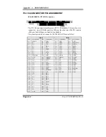
Page 94: ...RQ9 C4 LA22 D4 IRQ10 A5 D4 B5 5V C5 LA21 D5 IRQ11 A6 D3 B6 DRQ2 C6 LA20 D6 IRQ12 A7 D2 B7 12V C7 LA19 D7 IRQ15 A8 D1 B8 OWS C8 LA18 D8 IRQ14 A9 D0 B9 12V C9 LA17 D9 DACK0 A10 IOCHRDY B10 GND C10 MEMR D10 DRQ0 A11 AEN B11 SMEMW C11 MEMW D11 DACK5 A12 A19 B12 SMEMR C12 D8 D12 DRQ5 A13 A18 B13 IOW C13 D9 D13 DACK6 A14 A17 B14 IOR C14 D10 D14 DRQ6 A15 A16 B15 DACK3 C15 D11 D15 DACK7 A16 A15 B16 DRQ3 C...

Page 95: ...4 SD05 D4 IRQ11 C4 LA21 B5 5V A5 SD04 D5 IRQ12 C5 LA20 B6 DRQ2 A6 SD03 D6 IRQ15 C6 LA19 B7 12V A7 SD02 D7 IRQ14 C7 LA18 B8 OWS A8 SD01 D8 DACK0 C8 LA17 B9 12V A9 SD00 D9 DRQ0 C9 MEMR B10 GND A10 I O CH RDY D10 DACK5 C10 MEMW B11 SMEMW A11 AEN D11 DRQ5 C11 SD08 B12 SMEMR A12 SA19 D12 DACK6 C12 SD09 B13 IOW A13 SA18 D13 DRQ6 C13 SD10 B14 IOR A14 SA17 D14 DACK7 C14 SD11 B15 DACK3 A15 SA16 D15 DRQ7 C1...

Page 96: ...E37 GND F8 INTD E8 5V F38 GND E38 STOP F9 REQ3 E9 CLKC F39 LOCK E39 3 3V F10 REQ1 E10 5V I O F40 PERR E40 SDONE F11 GNT3 E11 CLKD F41 3 3V E41 SB0 F12 GND E12 GND F42 SERR E42 GND F13 GND E13 GND F43 3 3V E43 PAR F14 CLKA E14 GNT1 F44 C BE1 E44 AD15 F15 GND E15 RST F45 AD14 E45 3 3V F16 CLKB E16 5V I O F46 GND E46 AD13 F17 GND E17 GNT0 F47 AD12 E47 AD11 F18 REQ0 E18 GND F48 AD10 E48 GND F19 5V I O...

Page 97: ...Page B 1 TECHNICAL SUMMARY This section introduces you the maps concisely Section includes Block Diagram Interrupt Map RTC CMOS RAM Map Timer DMA Channels Map I O Memory Map APPENDIX B ...

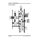
Page 98: ...Appendix B Technical Summary Page B 2 Prox 1550 USER S MANUAL BLOCK DIAGRAM ...

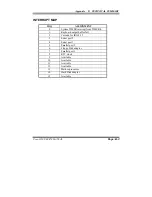
Page 99: ...System TIMER interrupt from TIMER 0 1 Keyboard output buffer full 2 Cascade for IRQ 8 15 3 Serial port 2 4 Serial port 1 5 Parallel port 2 6 Floppy Disk adapter 7 Parallel port 1 8 RTC clock 9 Available 10 Available 11 Available 12 Available 13 Math coprocessor 14 Hard Disk adapter 15 Available ...

Page 100: ...0C Status register C 0D Status register D 0E Diagnostic status byte 0F Shutdown byte 10 Floppy Disk drive type byte 11 Reserve 12 Hard Disk type byte 13 Reserve 14 Equipment byte 15 Base memory low byte 16 Base memory high byte 17 Extension memory low byte 18 Extension memory high byte 30 Reserved for extension memory low byte 31 Reserved for extension memory high byte 32 Date Century byte 33 Info...

Page 101: ...imer Channel Map Timer Channel Assignment 0 System timer interrupt 1 DRAM Refresh request 2 Speaker tone generator DMA Channel Map DMA Channel Assignment 0 Available 1 IBM SDLC 2 Floppy Disk adapter 3 Channel 3 Available 4 Cascade for DMA controller 1 5 Available 6 Available 7 Available ...

Page 102: ... MAP ASSIGNMENT 000 01F DMA controller Master 020 021 Interrupt controller Master 022 023 Chipset controller registers I O ports 040 05F Timer control regsiters 060 06F Keyboard interface controller 8042 070 07F RTC ports CMOS I O ports 080 09F DMA register 0A0 0BF Interrupt controller Slave 0C0 0DF DMA controller Slave 0F0 0FF Math coprocessor 1F0 1F8 Hard Disk controller 278 27F Parallel port 2 ...

Page 103: ...This section outlines the error message may occur when you operate the system also gives you the suggestions on solving the problems Section includes Trouble Shooting for Error Messages Trouble Shooting for POST Code APPENDIX C ...

Page 104: ...curred This beep code consists of a single long beep repeatedly CMOS BATTERY FAILURE When the CMOS battery is out of work or has run out the user has to replace the whole unit CMOS CHECKSUM ERROR This error message informs you that the CMOS is corrupted When the battery runs weak this situation might happen Please check the battery and change a new one when necessary DISPLAY SWITCH IS SET INCORREC...

Page 105: ... find or initialize the floppy drive controller please check the controller whether in proper Setup If there are no floppy drive installed Ensure the Diskette Drive selection in Setup is set to NONE KEYBOARD ERROR OR NO KEYBOARD PRESENT When this situation happens please check keyboard attachment and no keys being pressed during the boot If you are purposely configuring the system without a keyboa...

Page 106: ...d and the system must be rebooted Press and hold down the CTRL and ALT keys and press DEL TROUBLE SHOOTING FOR POST CODES When you power on your computer system and the screen display nothing You have to insert the POST Card for test The address for ISA POST port is 80h Make sure the card is in correct slot The lists below indicate you the error messages Please follow the instruction to adjust you...

Page 107: ...nding Interrupt handlers Initialize INT no from 33 120 with Dummy Spurious Interrupt Handler 2 Issue CPUID instruction to identify CPU type 3 Early Power Management initialization OEM specific 0B 1 Verify the RTC time is valid or not 2 Detect bad battery 3 Read CMOS data into BIOS stack area 4 PnP initializations including PnP BIOS only Assign CSN to PnP ISA card Create resource map from ESCD 5 As...

Page 108: ...hannel 1 test 11 DMA page registers test 14 Test 8254 Timer 0 Counter2 15 Test 8259 interrupt mask bits for channel 1 16 Test 8259 interrupt mask bits for channel 2 19 Test 8259 functionality 30 Detect Base Memory Extended Memory Size 31 1 Test Base Memory from 256K to 640K 2 Test Extended Memory from 1M to the top of memory 32 1 Display the Award Plug Play BIOS Extension message PnP BIOS only 2 P...

Page 109: ... ports 45 Initialize math coprocessor 4E If there is any error detected such as video kb show all the error messages the screen wait for user to press F1 key 4F 1 If password is needed ask for password 2 Clear the Energy Star Logo Green BIOS only 50 Write all CMOS values currently in the BIOS stack area back into the CMOS 52 1 Initialize all ISA ROMs 2 Later PCI initializations PCI BIOS only assig...

Page 110: ...kipped 2 Set the boot up speed according to Setup setting 3 Last chance for Chipset initialization 4 Last chance for Power Management initialization Green BIOS only 5 Show the system configuration table 62 1 Setup daylight saving according to Setup value 2 Program the NumLock typematic rate typematic speed according to Setup setting 63 1 If there is any changes in the hardware configuration update...

Reviews: