background image

Appendix  A  System  Diagrams 


SP-7145/7147 SERIES USER MANUAL


Page: A-22


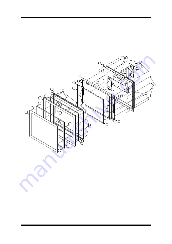
SP-7147 Touch Panel & LCD Display Exploded Diagram 


The  exploded  diagram  and  part  numbers  applies  to  SP-7147  system 

equipped with the following feature: 


Projected capacitive touch screen (DC-IN: 9-36V or 12V) 


06

13

12

01

09

08

02

17

17

17

12

14

09

08

17

17

17

17

17

11

10

17

04

07

03

17

15

16

05

17

17

17

17

17

17

11

10

17

04

17

17

Summary of Contents for SP-7145

Page 1: ...USER MANUAL SP 7145 7147 47 15 17 Fanless Panel PC Powered by Intel Atom E3845 Celeron J1900 CPU Processor With DVI I 3COM 4USB 2LAN SP 7145 7147 M2...

Page 2: ...ansmit in any form or by any means electronic or mechanical including photocopying and recording DISCLAIMER This user s manual is meant to assist users in installing and setting up the system The info...

Page 3: ...ser will be required to correct the interference at his own expense You are cautioned that any change or modifications to the equipment not expressly approve by the party responsible for compliance co...

Page 4: ...agram DC IN 9 36V 3 2 3 1 2 Rear I O Ports Diagram DC IN 12V 3 2 3 2 JUMPER CONNECTOR QUICK REFERENCE TABLE 3 2 3 3 COMPONENT LOCATIONS 3 3 3 3 1 Top View and Jumper Settings of SP 7145 7147 3 3 3 4 S...

Page 5: ...3 5 18 DIO WAFER optional 3 21 3 5 19 FRONT CONNECTOR 3 21 3 5 20 INVERTER WAFER 3 22 3 5 21 KB MS PORT 3 23 3 5 22 LAN USB2 0 PORT 3 24 3 5 23 LAN USB2 0 3 0 PORT 3 25 3 5 24 SATA CONNECTOR 3 27 3 5...

Page 6: ...00 CONNECTORS JUMPERS 3 39 3 11 1 VIN Connector 9V 36V 3 39 3 11 2 VOUT Connector 12V 3 39 3 11 3 RUN CONTROL INPUT SELECTION 3 40 3 11 4 PULSE SKIPPING MODE SELECTION 3 41 3 11 5 CONTINUOUS MODE SELE...

Page 7: ...ly 5 10 5 4 2 Advanced ACPI Settings 5 11 5 4 3 Advanced F81866 Super IO Configuration 5 12 5 4 4 Advanced Hardware Monitor 5 19 5 4 5 Advanced F81866 Watchdog Configuration 5 21 5 4 6 Advanced CPU Co...

Page 8: ...oded Diagram 17 SP 7145 HDD Tray Exploded Diagram 19 SP 7145 Panel Mount Exploded Diagram 20 SP 7147 System Exploded Diagram 21 SP 7147 Touch Panel LCD Display Exploded Diagram 22 SP 7147 Touch Panel...

Page 9: ...Location Top View 3 3 Figure 3 2 Daughter Board BR 6062 Component Location Top View 3 33 Figure 3 2 Daughter Board SR 6100 Component Location Top View 3 38 Figure 5 1 Extensible Firmware Interface Di...

Page 10: ...r Manual is described below Version No Revision History Date M1 Initial Release 2017 06 27 M2 1 SP 7145 7147 system diagrams have been changed 2 SP 7145 7147 rear I O ports diagrams have been changed...

Page 11: ...7147 SERIES USER MANUAL Page 1 1 1 Introduction This chapter provides the introduction for the SP 7145 7147 system as well as the framework of the user manual The following topic is included About Thi...

Page 12: ...physical illustrations for the SP 7145 7147 system Read the safety reminders carefully on how to take care of your system properly Chapter 3 System Configuration This chapter outlines the locations o...

Page 13: ...145 7147 system It describes how to set up the system quickly and outlines the system specifications The following topics are included Package List System Overview System Diagrams System Specification...

Page 14: ...L Page 2 2 2 1 Package List If you discover any of the items listed below are damaged or lost please contact your local distributor immediately Item Q ty SP 7145 7147 1 Manual Driver DVD 1 Quick Guide...

Page 15: ...Chapter 2 Getting Started SP 7145 7147 SERIES USER MANUAL Page 2 3 2 2 System Diagrams Unit mm SP 7145 Front View Rear View Top View...

Page 16: ...Chapter 2 Getting Started SP 7145 7147 SERIES USER MANUAL Page 2 4 Bottom View DC IN 9 36V DC IN 12V Unit mm Left Side View Right Side View...

Page 17: ...Chapter 2 Getting Started SP 7145 7147 SERIES USER MANUAL Page 2 5 Quarter View...

Page 18: ...Chapter 2 Getting Started SP 7145 7147 SERIES USER MANUAL Page 2 6 SP 7147 Unit mm Front View Rear View Top View...

Page 19: ...Chapter 2 Getting Started SP 7145 7147 SERIES USER MANUAL Page 2 7 Bottom View DC IN 9 36V DC IN 12V Unit mm Left Side View Right Side View...

Page 20: ...Chapter 2 Getting Started SP 7145 7147 SERIES USER MANUAL Page 2 8 Quarter View...

Page 21: ...x 320mm x 26mm SP 7147 7 9 kg 436mm x 368mm x 27 4mm Certificate CE FCC I O Ports Serial Port COM1 2 3 4 for RS 232 COM4 optional COM3 4 pin9 5V 12V RI selectable COM5 6 for RS 232 422 485 via daughte...

Page 22: ...ted resistive capacitive touch screen Environment Operating Temp with airflow HDD 0 C 40 C 32 F 104 F SSD 0 C 45 C 32 F 113 F Wide Temperature 0 C 50 C SSD with J1900 Sunlight readable panel 0 C 55 C...

Page 23: ...dly from a hot place to a cold place and vice versa because condensation may occur inside the system Protect your SP 7145 7147 from strong vibrations which may cause hard disk failure Do not place the...

Page 24: ...nd jumper connector settings and component locations for the main board and daughter board The following topics are included External I O Ports Diagram Main Board Jumper Settings and Component Locatio...

Page 25: ...tional Remote SW COM4 COM5 DIO DC IN 12V PS 2 LAN1 LAN2 Power COM6 COM2 COM1 Button COM3 DVI I USB2 0 2 0 USB2 0 3 0 DVI I USB Line out PS 2 Mouse Connector Mic in Keyboard Connector GND VCC PS 2 Mous...

Page 26: ...tion JP_COM4 Audio Port JAUDIO1 Battery Wafer JBAT1 COM Port JCOM2_3 COM4 Connector JCOM4 COM5 Connector JCOM5 COM6 Connector JCOM6 DVI I COM Port JCOM_DVII1 FAN Connector JCPU_FAN1 JSYS_FAN1 DC 12V C...

Page 27: ...P 7145 7147 Figure 3 1 Main Board Component Location Top View WARNING Always disconnect the power cord when you are working with connectors and jumpers on the main board Make sure both the system and...

Page 28: ...ic charge while you are working on the connectors and jumpers Use a grounding wrist strap and place all electronic components in any static shielded devices CAUTION Always touch the motherboard compon...

Page 29: ...gs by opening or closing jumpers Jumpers can be combined into sets that are called jumper blocks When jumpers are all in the block you have to put them together to set up the hardware configuration Th...

Page 30: ...Chapter 3 Hardware Configuration SP 7145 7147 SERIES USER MANUAL Page 3 6 Jumper diagrams Jumper settings...

Page 31: ...e 3 7 3 5 Setting Main Board Connectors and Jumpers 3 5 1 LVDS POWER SELECTION JP4 LVDS Power Selection SELECTION JUMPTER SETTING JUMPER ILLUSTRATION 3 3V 1 2 3 1 JP4 5V 2 3 3 1 JP4 Note Manufacturing...

Page 32: ...3 5 2 BACKLIGHT INVERTER PWM VOLTAGE SELECTION JP5 Backlight Inverter PWM Voltage Selection SELECTION JUMPTER SETTING JUMPER ILLUSTRATION 3 3V 1 2 3 1 JP5 5V 2 3 3 1 JP5 GND NC 3 1 JP5 Note Manufactu...

Page 33: ...JP7 Power On Mode Selection SELECTION JUMPTER SETTING JUMPER ILLUSTRATION Auto on 1 2 1 JP7 Select by BIOS NC 1 JP7 Note 1 Manufacturing default is Auto on Note 2 Manufacturing default for BS H292 SBO...

Page 34: ...USER MANUAL Page 3 10 3 5 4 BACKLIGHT ENABLE SELECTION JP9 BACKLIGHT ENABLE Selection SELECTION JUMPTER SETTING JUMPER ILLUSTRATION 5V 2 3 1 3 JP9 3 3V 1 2 1 3 JP9 Note Manufacturing default for SP 7...

Page 35: ...ration SP 7145 7147 SERIES USER MANUAL Page 3 11 3 5 5 VGA DVI SELECTION JP10 VGA DVI Selection SELECTION JUMPTER SETTING JUMPER ILLUSTRATION DVI 1 3 5 6 5 6 1 2 JP10 VGA 1 2 4 6 5 6 1 2 JP10 Note Man...

Page 36: ...SOLUTION SELECTION JP14 JP15 LVDS Resolution Selection SELECTION JUMPTER SETTING JUMPER ILLUSTRATION 1024x768 1CH 24bit for SP 7145 JP15 4 6 JP15 3 5 JP14 2 4 JP14 3 5 5 6 1 2 JP14 5 6 1 2 JP15 1280x1...

Page 37: ...ER MANUAL Page 3 13 3 5 7 COM3 PIN9 DEFINITION SELECTION GUIDE JP_COM3 COM3 Port pin9 RI 5V 12V Selection SELECTION JUMPTER SETTING JUMPER ILLUSTRATION RI 1 2 5 6 1 2 JP_COM3 12V 3 4 5 6 1 2 JP_COM3 5...

Page 38: ...14 3 5 8 COM4 VOLTAGE SELECTION JP_COM4 COM4 Voltage Selection SELECTION JUMPTER SETTING JUMPER ILLUSTRATION RI 1 2 2 1 6 5 JP_COM4 12V 3 4 2 1 6 5 JP_COM4 5V 5 6 2 1 6 5 JP_COM4 Note 1 Manufacturing...

Page 39: ...phone The connector can also support only Microphone Line In PIN ASSIGNMENT 32 LINE IN L 33 NC 34 NC 35 LINE IN R Line Out PIN ASSIGNMENT 22 LINE OUT L 23 NC 24 NC 25 LINE OUT R Mic In PIN ASSIGNMENT...

Page 40: ...7145 7147 SERIES USER MANUAL Page 3 16 3 5 10 BATTERY WAFER JBAT1 Battery Wafer PIN ASSIGNMENT 1 RTC_BAT 2 GND 3 5 11 COM2 and COM3 PORTS JCOM2_3 COM Port PIN ASSIGNMENT 1 DCD 2 RXD 3 TXD 4 DTR 5 GND...

Page 41: ...r 3 Hardware Configuration SP 7145 7147 SERIES USER MANUAL Page 3 17 3 5 12 COM4 CONNECTOR JCOM4 COM4 Connector PIN ASSIGNMENT PIN ASSIGNMENT 1 DCD 6 DSR 2 RXD 7 RTS 3 TXD 8 CTS 4 DTR 9 RI 5 GND 10 NC...

Page 42: ...3 5 13 COM5 CONNECTOR JCOM5 COM5 Connector PIN ASSIGNMENT PIN ASSIGNMENT 1 DCD 6 DSR 2 RXD 7 RTS 3 TXD 8 CTS 4 DTR 9 RI 5 GND 10 NC 3 5 14 COM6 CONNECTOR JCOM6 COM6 Connector PIN ASSIGNMENT PIN ASSIGN...

Page 43: ...ENT PIN ASSIGNMENT 1 TMDS_D2 2 TMDS_D2 3 GND 4 NC 5 NC 6 DDC_CLK 7 DDC_DATA 8 VSYNC 9 TMDS_D1 10 TMDS_D1 11 GND 12 NC 13 NC 14 5V 15 GND 16 HPD 17 TMDS_D0 18 TMDS_D0 19 GND 20 NC 21 NC 22 GND 23 TMDS_...

Page 44: ...S USER MANUAL Page 3 20 3 5 16 FAN CONNECTOR JCPU_FAN1 JSYS_FAN1 Fan Connector PIN ASSIGNMENT 1 GND 2 12V 3 FAN_CONTROL 4 FAN_SIGNAL 3 5 17 DC 12V CONNECTOR JDC_PWR1 DC 12V Connector PIN ASSIGNMENT 1...

Page 45: ...GNMENT PIN ASSIGNMENT 1 5V 6 GND 2 DIN0 7 DOUT0 3 DIN1 8 DOUT1 4 DIN2 9 DOUT2 5 DIN3 10 DOUT3 3 5 19 FRONT CONNECTOR JFP1 Front Connector PIN ASSIGNMENT PIN ASSIGNMENT 1 HDD_LED 7 RESET SWITCH 2 PWR_L...

Page 46: ...Chapter 3 Hardware Configuration SP 7145 7147 SERIES USER MANUAL Page 3 22 3 5 20 INVERTER WAFER JINV1 Inverter Wafer PIN ASSIGNMENT 1 12V 2 12V 3 GND 4 PWM SIGNAL 5 GND 6 BACKLIGHT EN JINV1...

Page 47: ...P 7145 7147 SERIES USER MANUAL Page 3 23 3 5 21 KB MS PORT JKB_MS1 KB MS Port Keyboard PIN ASSIGNMENT 1 DATA 2 NC 3 GND 4 5V 5 CLK 6 NC Mouse PIN ASSIGNMENT 7 DATA 8 NC 9 GND 10 5V 11 CLK 12 NC 3 1 2...

Page 48: ...5 7147 SERIES USER MANUAL Page 3 24 3 5 22 LAN USB2 0 PORT JLAN_USB1 LAN USB2 0 PORT LAN PIN ASSIGNMENT 1 TX_D1 2 TX_D1 3 RX_D2 4 BI_D3 5 BI_D3 6 RX_D2 7 BI_D4 8 BI_D4 Yellow Orange Green JLAN_USB1 US...

Page 49: ...LAN USB2 0 3 0 PORT JLAN_USB2 LAN USB2 0 3 0 PORT LAN PIN ASSIGNMENT 1 TX_D1 2 TX_D1 3 RX_D2 4 BI_D3 5 BI_D3 6 RX_D2 7 BI_D4 8 BI_D4 USB2 0 PIN ASSIGNMENT B1 VBUS B2 D B3 D B4 GND B5 STDA_SSRX B6 STD...

Page 50: ...MENT 1 LVDS_VCC 2 GND 3 LVDS1_CLK 4 LVDS1_CLK 5 GND 6 LVDS1_D2 7 LVDS1_D2 8 GND 9 LVDS1_D1 10 LVDS1_D1 11 LVDS1_D3 12 LVDS1_D3 13 LVDS1_D0 14 LVDS1_D0 15 GND 16 LVDS0_CLK 17 LVDS0_CLK 18 GND 19 LVDS0_...

Page 51: ...3 27 3 5 24 SATA CONNECTOR JSATA1 JSATA2 Two Serial ATA Connectors PIN ASSIGNMENT 1 GND 2 TX 3 TX 4 GND 5 RX 6 RX 7 GND 2 30 SATA POWER CONNECTOR JSATA_PWR1 JSATA_PWR2 SATA Power Connector PIN ASSIGNM...

Page 52: ...hapter 3 Hardware Configuration SP 7145 7147 SERIES USER MANUAL Page 3 28 3 5 25 USB CONNECTOR JUSB1 USB Connector PIN ASSIGNMENT PIN ASSIGNMENT 1 5V 2 5V 3 D 4 D 5 D 6 D 7 GND 8 GND 9 GND 10 GND JUSB...

Page 53: ...3 NC 4 GND 5 NC 6 1 5V 7 CLKREQ 8 NC 9 GND 10 NC 11 REFCLK 12 NC 13 REFCLK 14 NC 15 GND 16 NC 17 NC 18 GND 19 NC 20 NC 21 GND 22 PERST 23 PERn0 24 3 3V 25 PERp0 26 GND 27 GND 28 1 5V 29 GND 30 SMB_CL...

Page 54: ...PIN ASSIGNMENT A1 NC B1 12V A2 12V B2 12V A3 12V B3 12V A4 GND B4 GND A5 NC B5 SMB_CLK A6 NC B6 SMB_DATA A7 NC B7 GND A8 NC B8 3 3V A9 3 3V B9 NC A10 3 3V B10 3 3V_SB A11 PWRGD B11 WAKE A12 GND B12 N...

Page 55: ...UAL Page 3 31 3 5 28 LPC CONNECTOR JLPC1 LPC Connector PIN ASSIGNMENT PIN ASSIGNMENT 1 CLK 2 GND 3 FRAME 4 NC 5 RESET 6 VCC5 7 LAD3 8 LAD2 9 VCC3 10 LAD1 11 LAD0 12 GND 13 SMBCLK 14 SMBDATA 15 3VSB 16...

Page 56: ...tep 2 Close JP1 pins 1 2 for 6 seconds by a cap Step 3 Remove the cap which is just used on JP1 1 2 so that JP1 returns to OPEN Step 4 Power on the PC and the PC will then auto reboot for once in orde...

Page 57: ...er Board with 2UART to RS 232 422 485 Transceiver JUMPER NAME JP1 RS 485 Auto Flow Control for JCOM1_1 JCOM1 JP2 RS 232 422 485 Selection for JCOM1_1 JCOM1 JP3 RS 485 Auto Flow Control for JCOM2_1 JP3...

Page 58: ...ANUAL Page 3 34 3 8 SETTING DAUGHTER BOARD BR 6062 JUMPERS 3 8 1 RS 485 AUTO FLOW CONTROL FOR JCOM1_1 JCOM1 JP1 RS 485 Auto Flow Control Selection for JCOM1_1 and JCOM1 SELECTION JUMPTER SETTING JUMPE...

Page 59: ...47 SERIES USER MANUAL Page 3 35 3 8 2 RS 232 422 485 SELECTION FOR JCOM1_1 JCOM1 JP2 RS 232 422 485 Selection for JCOM1_1 JCOM1 Selection Jumper Setting Jumper Illustration RS 232 Default Open JP2 RS...

Page 60: ...ion SP 7145 7147 SERIES USER MANUAL Page 3 36 3 8 3 RS 485 AUTO FLOW CONTROL FOR JCOM2_1 JP3 RS 485 Auto Flow Control Selection for JCOM2_1 SELECTION JUMPTER SETTING JUMPER ILLUSTRATION Normal Default...

Page 61: ...145 7147 SERIES USER MANUAL Page 3 37 3 8 4 RS 232 422 485 SELECTION FOR JCOM2_1 JP4 RS 232 422 485 Selection for JCOM2_1 Selection Jumper Setting Jumper Illustration RS 232 Default Open JP4 RS 422 1...

Page 62: ...er Board with 2UART to RS 232 422 485 Transceiver JUMPER NAME JP1 Run Control Output Selection JP2 JP3 Pulse Skipping Mode Selection JP2 JP3 Continuous Mode Selection CONNECTOR NAME VIN VIN Voltage Se...

Page 63: ...SER MANUAL Page 3 39 3 11 SETTING DAUGHTER BOARD SR 6100 CONNECTORS JUMPERS 3 11 1 VIN Connector 9V 36V VIN VIN Connector PIN ASSIGNMENT 1 VIN 2 VIN 3 GND 4 GND 3 11 2 VOUT Connector 12V VIN VIN Conne...

Page 64: ...Configuration SP 7145 7147 SERIES USER MANUAL Page 3 40 3 11 3 RUN CONTROL INPUT SELECTION JP1 Run Control Input Selection SELECTION JUMPTER SETTING JUMPER ILLUSTRATION VIN Turn On Default 1 2 JP1 GND...

Page 65: ...E SELECTION JP2 JP3 Pulse Skipping Mode Selection SELECTION JUMPTER SETTING JUMPER ILLUSTRATION Pulse Skipping Mode Default 1 2 JP2 NC Open JP3 3 11 5 CONTINUOUS MODE SELECTION JP2 JP3 Continuous Mode...

Page 66: ...ng topics are included Installing Intel Chipset Software Installation Utility Installing Intel Trusted Execution Engine Interface Installing Graphics Driver Utility Installing LAN Driver Utility Insta...

Page 67: ...er installation X D Driver Platform USB3 0 Intel R USB 3 0 eXtensible Host Controller Utility X D Driver Platform Sound Codec Realtek ALC888S For Sound driver installation X D Driver Platform Windows...

Page 68: ...ed Capacitive touch driver installation X For WES7 only X Not support Support Note Install the driver utilities immediately after the OS installation is completed Filename Assume that DVD ROM drive is...

Page 69: ...allation Utility X D Driver Platform TXE For Intel Trusted Execution Engine Interface X D Driver Platform Graphics Intel HD Graphics X D Driver Platform LAN Chip Intel I210 IT For LAN Driver installat...

Page 70: ...omponents in the Device Manager 4 2 2 Intel Chipset Software Installation Utility The utility pack is to be installed only for Windows 7 10 series and it should be installed immediately after the OS i...

Page 71: ...k KMDF follow the steps below 1 Insert the driver disk into a DVD ROM device 2 For Windows 7 only Enter the KMDF folder where the installation driver file is located 3 For Windows 7 only Click the Set...

Page 72: ...and make the system work simultaneously To install the Graphics driver utility follow the steps below 1 Connect the USB DVD ROM device to SP 7145 7147 and insert the driver disk 2 Enter the Graphics...

Page 73: ...iver disk 2 Enter the LAN folder where the driver is located 3 Select Windows 7 32 64 bit Windows 10 32 64 bit for your OS platform 4 Click the LAN driver installation file for driver installation 5 F...

Page 74: ...reTM Processors Intel C610 series Chipset Family Intel 9 Series Chipset Family Intel Pentium Processor or Intel Celeron Processor N J Series Intel 5th generation Intel CoreTM Processors Intel CoreTM M...

Page 75: ...n screen instructions to complete the installation 6 Once the installation is completed shut down the system and restart SP 7145 7147 for the changes to take effect 4 8 Installing Resistive Touch Driv...

Page 76: ...DVD ROM device to SP 7145 7147 and insert the driver disk 2 Enter the Touch driver WES7 folder where the driver is located 3 Select WES 7 32 64 bit for your OS platform 4 Click the Touch driver insta...

Page 77: ...put System Setup Utilities The information of the system configuration is saved in battery backed CMOS RAM and BIOS NVRAM so that the Setup information is retained when the system is powered off The B...

Page 78: ...I Unified Extensible Firmware Interface specifications and the Intel Platform Innovation Framework for EFI The UEFI specification defines an interface between the operating system and platform firmwar...

Page 79: ...stem and allows technicians to troubleshoot the occurred errors when the hardware is faulty The BIOS setup menu allows users to view and modify the BIOS settings for the computer After the system is p...

Page 80: ...etup SP 7145 7147 SERIES USER MANUAL Page 5 4 Figure 5 2 POST Screen with AMI Logo Press Del or Esc to access the Setup Utility program and the Main menu of the Aptio Setup Utility will appear on the...

Page 81: ...item a brief description of the highlighted selection will appear on the right side of the screen The language of the BIOS setup menu interface and help messages are shown in US English You may use o...

Page 82: ...BIOS setup menu BIOS Messages This section describes the alert messages generated by the board s BIOS These messages would be shown on the monitor when certain recoverable errors events occur during...

Page 83: ...ld Date and Time Main Screen BIOS Setting Options Description Purpose BIOS Vendor No changeable options Displays the BIOS vendor Core Version No changeable options Displays the current BIOS core versi...

Page 84: ...age English BIOS Setup language System Date Month day year Sets the system date The format is Day Month Date Year Users can directly enter values or use or arrow keys to increase decrease it The Day i...

Page 85: ...uration Advanced Menu Screen BIOS Setting Options Description Purpose Trusted Computing Sub Menu Trusted Computing Parameters BayTrail I only ACPI Settings Sub Menu System ACPI Parameters F81866 Super...

Page 86: ...s users to enable disable BIOS support for security device The operating system will not show Security Device The TCG EFI protocol and INT1A interface will not be available Trusted Computing Configura...

Page 87: ...PI Settings allows users to configure relevant ACPI Advanced Configuration and Power Management Interface settings such as Enable Disable ACPI Auto Configuration Enable Disable Hibernation ACPI Sleep...

Page 88: ...ock Legacy Resources Disabled Enabled Enables or Disables Lock of Legacy Resources 5 4 3 Advanced F81866 Super IO Configuration Menu Path Advanced F81866 Super IO Configuration F81866 Super IO Configu...

Page 89: ...OMD Serial Port 5 Configuration Sub menu Sets the parameters of Serial Port 5 COME Serial Port 6 Configuration Sub menu Sets the parameters of Serial Port 6 COMF Menu Path Advanced F81866 Super IO Con...

Page 90: ...1 Menu Path Advanced F81866 Super IO Configuration Serial Port 2 Configuration Serial Port 2 Configuration Screen BIOS Setting Options Description Purpose Serial Port Disabled Enabled Enables or Disab...

Page 91: ...escription Purpose Serial Port Disabled Enabled Enables or Disables Serial Port 3 Device Settings No changeable options Displays the current settings of Serial Port 3 Change Settings IO 3E8h IRQ 10 IO...

Page 92: ...Description Purpose Serial Port Disabled Enabled Enables or Disables Serial Port 4 Device Settings No changeable options Displays the current settings of Serial Port 4 Change Settings IO 2E8h IRQ 5 IO...

Page 93: ...Description Purpose Serial Port Disabled Enabled Enables or Disables Serial Port 5 Device Settings No changeable options Displays the current settings of Serial Port 5 Change Settings IO 2F0h IRQ 7 IO...

Page 94: ...scription Purpose Use This Device Disabled Enabled Enables or Disables Serial Port 6 Device Settings No changeable options Displays the current settings of Serial Port 6 Change Settings IO 2E0h IRQ 7...

Page 95: ...levels in supply Hardware Monitor Screen BIOS Setting Options Description Purpose Smart CPU FAN Auto Disabled Manual Adjusts Smart CPU Fan Start Boundary Temperature 20 60 Adjusts Smart Boundary Tempe...

Page 96: ...e segment speed will set 60 70 80 90 100 Segment Speed Count Step 5 10 Adjust Segment Speed Count Step CPU Temperature No changeable options Displays the processor s temperature System Temperature No...

Page 97: ...rigger a system reset via the 255 level watchdog timer F81866 Watchdog Configuration Screen BIOS Setting Options Description Purpose Enable Watchdog Enabled Disabled Enables Disables F81866 Watchdog t...

Page 98: ...Screen BIOS Setting Options Description Purpose Socket 0 CPU Information Sub Menu Reports CPU Information CPU Speed No changeable options Reports the current CPU Speed 64 bit No changeable options Rep...

Page 99: ...Microcode Patch Version Max CPU Speed No changeable options Reports the maximum CPU Speed Min CPU Speed No changeable options Reports the minimum CPU Speed Processor Cores No changeable options Displa...

Page 100: ...NUAL Page 5 24 BIOS Setting Options Description Purpose L1 Code Cache No changeable options Displays L1 Code Cache size L2 Cache No changeable options Displays L2 Cache size L3 Cache No changeable opt...

Page 101: ...indicates the functions available when the SATA controller is enabled and the AHCI mode is selected IDE Configuration Screen BIOS Setting Options Description Purpose Serial ATA Controller s Disabled...

Page 102: ...1 Disabled Enabled Enables or disables SATA port 0 Device Serial ATA Port 1 Note 2 Disabled Enabled Enables or disables SATA port 1 Device SATA Port 0 drive Displays the drive installed on this SATA...

Page 103: ...Advanced CSM Configuration The CSM Configuration provides advanced CSM Compatibility Support Module configurations such as Enable Disable CSM Support configure Option ROM execution boot option filter...

Page 104: ...Trail D only Boot option filter UEFI and Legacy Legacy only UEFI only This option controls what kind of devices system can boot Network Do not launch UEFI only Legacy only Controls the execution of UE...

Page 105: ...ions Description Purpose USB Devices No changeable options Displays the number of available USB devices Legacy USB Support Disabled Enabled Auto Enables support for legacy USB XHCI Hand off Disabled E...

Page 106: ...t 10 20 30 40 sec USB mass storage device Start Unit command time out Device power up delay Auto Manual The maximum time the device will take before it properly reports itself to the Host Controller A...

Page 107: ...lows users to configure advanced Chipset settings such as North Bridge and South Bridge configuration parameters Chipset Screen BIOS Setting Options Description Purpose North Bridge Sub menu Sets Para...

Page 108: ...n the platform North Bridge Screen BIOS Setting Options Description Purpose LCD Control Sub menu LCD Control Settings BayTrail I only Intel IGD Configuration Sub menu Configure Graphic Settings BayTra...

Page 109: ...Chapter 5 BIOS Setup SP 7145 7147 SERIES USER MANUAL Page 5 33 BayTrail D...

Page 110: ...Intel IGD Configuration No changeable options Displays the IGD information on platform Integrated Graphics Device Disabled Enabled Enabled Enable Integrated Graphics Device IGD when selected as the P...

Page 111: ...e LCD Control BayTrail I only The LCD Control allows users to select the primary display device LCD Control Screen BIOS Setting Options Description Purpose Primary IGFX Boot Display VBIOS Default CRB...

Page 112: ...E parameters BayTrail D only High Precision Timer Disabled Enabled Enables or disables the HPET High Precision Event Timer BayTrail D only Restore AC Power Loss Power Off Power On Last State Selects A...

Page 113: ...Chapter 5 BIOS Setup SP 7145 7147 SERIES USER MANUAL Page 5 37 BayTrail I SoC...

Page 114: ...u Path Chipset South Bridge Azalia HD Audio The Azalia HD Audio allows users to controls the detection of the Azalia device Azalia HD Audio Screen BIOS Setting Options Description Purpose Audio Contro...

Page 115: ...anagement Disabled Enabled Enables Disables USB2 Link Power Management BayTrail D only USB 2 0 EHCI Support Disabled Enabled Users needs to disable XHCI Mode Enables Enhanced Host Controller Interface...

Page 116: ...7147 SERIES USER MANUAL Page 5 40 BIOS Setting Options Description Purpose Enabled USB Hub 1 4 USB Port 2 Disabled Enabled Enabled or Disabled USB port 2 USB Port 3 Disabled Enabled Enabled or Disabl...

Page 117: ...il D only PCI Express Port Configuration Screen BIOS Setting Options Description Purpose PCI Express Port Disabled Enabled Enables or Disables PCI Express port Speed Auto Gen1 Gen2 Selects PCI Express...

Page 118: ...sers from changing your BIOS settings You can configure an Administrator password and then configure a user password An administrator has much more privileges over the settings in the Setup utility th...

Page 119: ...rd User Password option from the Security menu and press Enter and the password dialog entry box appears 2 Select the Administrator Password or User Password that you want to change A password can be...

Page 120: ...changing the boot order from the available bootable device s Boot Screen BIOS Setting Options Description Purpose Setup Prompt Timeout Numeric Number of seconds to wait for setup activation key Bootu...

Page 121: ...s Sub Menu Allow user to select boot order of available drive s Network Drive BBS Priorities Sub Menu Allow user to select boot order of available drive s Boot Hard Drive BBS Priorities Hard Drive BBS...

Page 122: ...SP 7145 7147 SERIES USER MANUAL Page 5 46 Boot Network Drive BBS Priorities Network Drive BBS Priorities BIOS Setting Options Description Purpose Boot Option 1 n Drive s Disabled Change the boot order...

Page 123: ...then exit the system Select Save Changes and Reset to validate the changed BIOS settings and then restart the system Discard Changed BIOS Settings To cancel the BIOS settings you have previously confi...

Page 124: ...tions Exits the system without saving any changes configured in BIOS settings Save Changes and Reset No changeable options Saves the changes in NVRAM and resets the system Discard Changes and Reset No...

Page 125: ...included SP 7145 System Exploded Diagram SP 7145 Touch Panel LCD Display Exploded Diagram SP 7145 Box PC Exploded Diagram SP 7145 HDD Tray Exploded Diagram SP 7145 Panel Mount Exploded Diagram SP 714...

Page 126: ...system equipped with the following features Resistive touch screen DC IN 9 36V or 12V Projected capacitive touch screen DC IN 9 36V or 12V No Component Name P N No Q ty 1 SP 7145_PANEL_SUS_EXP SEE PAG...

Page 127: ...Panel LCD Display Exploded Diagram The exploded diagram and part numbers applies to SP 7145 system equipped with the following feature Projected capacitive touch screen DC IN 9 36V 06 13 12 01 09 02 0...

Page 128: ...2 380 00075014 1 7 15 TFT LCD Panel LED Backlight 450 nits HD 1024x768 52 351 03006802 1 8 SP 7145 TOUCH THIN GAP EPDM H 370x5x3mm 30 013 01100411 2 9 SP 7145 TOUCH THIN GAP EPDM V 274x5x3mm 30 013 01...

Page 129: ...Panel LCD Display Exploded Diagram The exploded diagram and part numbers applies to SP 7145 system equipped with the following feature Projected capacitive touch screen DC IN 12V 06 13 12 01 09 02 08...

Page 130: ...15 TFT LCD Panel LED Backlight 450 nits HD 1024x768 52 351 03006802 1 8 SP 7145 TOUCH THIN GAP EPDM H 370x5x3mm 30 013 01100411 2 9 SP 7145 TOUCH THIN GAP EPDM V 274x5x3mm 30 013 01200411 2 10 SP 7145...

Page 131: ...ouch Panel LCD Display Exploded Diagram The exploded diagram and part numbers applies to SP 7145 system equipped with the following feature Resistive touch screen DC IN 9 36V 06 13 12 01 09 02 08 16 1...

Page 132: ...7 15 TFT LCD Panel LED Backlight 450 nits HD 1024x768 52 351 03006802 1 8 SP 7145 TOUCH THIN GAP EPDM H 370x5x3mm 30 013 01100411 2 9 SP 7145 TOUCH THIN GAP EPDM V 274x5x3mm 30 013 01200411 2 10 SP 7...

Page 133: ...Touch Panel LCD Display Exploded Diagram The exploded diagram and part numbers applies to SP 7145 system equipped with the following feature Resistive touch screen DC IN 12V 06 13 12 01 09 02 08 16 11...

Page 134: ...7 15 TFT LCD Panel LED Backlight 450 nits HD 1024x768 52 351 03006802 1 8 SP 7145 TOUCH THIN GAP EPDM H 370x5x3mm 30 013 01100411 2 9 SP 7145 TOUCH THIN GAP EPDM V 274x5x3mm 30 013 01200411 2 10 SP 7...

Page 135: ...11 SP 7145 Box PC Exploded Diagram The exploded diagram and part numbers applies to SP 7145 system equipped with the following feature Projected capacitive touch screen DC IN 9 36V 18 01 08 08 06 02...

Page 136: ...HEAD SCREW M3x0 5Px5mm 22 230 30005811 8 9 HEX CU BOSS UNC No 4 40 L 4 8 H 7mm 22 692 40048051 16 10 ROUND WASHER HEAD SCREW M3x0 5Px5mm 22 242 30005311 1 11 SP 7147 REMOTE SWITCH CABLE L 390mm 190mm...

Page 137: ...A 13 SP 7145 Box PC Exploded Diagram The exploded diagram and part numbers applies to SP 7145 system equipped with the following feature Projected capacitive touch screen DC IN 12V 18 01 08 08 06 02 1...

Page 138: ...D SCREW M3x0 5Px5mm 22 230 30005811 8 9 HEX CU BOSS UNC No 4 40 L 4 8 H 7mm 22 692 40048051 16 10 ROUND WASHER HEAD SCREW M3x0 5Px5mm 22 242 30005311 1 11 SP 7147 REMOTE SWITCH CABLE L 390mm 190mm 27...

Page 139: ...age A 15 SP 7145 Box PC Exploded Diagram The exploded diagram and part numbers applies to SP 7145 system equipped with the following feature Resistive touch screen DC IN 9 36V 18 01 08 06 18 02 08 07...

Page 140: ...HEAD SCREW M3x0 5Px5mm 22 230 30005811 8 9 HEX CU BOSS UNC No 4 40 L 4 8 H 7mm 22 692 40048051 16 10 ROUND WASHER HEAD SCREW M3x0 5Px5mm 22 242 30005311 1 11 SP 7147 REMOTE SWITCH CABLE L 390mm 190mm...

Page 141: ...Page A 17 SP 7145 Box PC Exploded Diagram The exploded diagram and part numbers applies to SP 7145 system equipped with the following feature Resistive touch screen DC IN 12V 18 01 08 06 02 18 03 09 1...

Page 142: ...D SCREW M3x0 5Px5mm 22 230 30005811 8 9 HEX CU BOSS UNC No 4 40 L 4 8 H 7mm 22 692 40048051 16 10 ROUND WASHER HEAD SCREW M3x0 5Px5mm 22 242 30005311 1 11 SP 7147 REMOTE SWITCH CABLE L 390mm 190mm 27...

Page 143: ...IN 9 36V or 12V No Component Name P N No Q ty 1 PK 7090 HDD SUPPORT BRACKET 20 006 03006284 1 2 PK 7090 HDD BRACKET 20 006 03005284 1 3 SP 7625 HDD BRACKET FIX PLATE 80 006 03011328 1 4 RUBBER WASHER...

Page 144: ...NUAL Page A 20 SP 7145 Panel Mount Exploded Diagram The exploded diagram and part numbers below applies to SP 7145 system equipped with the following features Resistive touch screen DC IN 9 36V or 12V...

Page 145: ...stem equipped with the following features Resistive touch screen DC IN 9 36V or 12V Projected capacitive touch screen DC IN 9 36V or 12V No Component Name P N No Q ty 1 SP 7147_PANEL_MODULE_EXP SEE PA...

Page 146: ...lay Exploded Diagram The exploded diagram and part numbers applies to SP 7147 system equipped with the following feature Projected capacitive touch screen DC IN 9 36V or 12V 06 13 12 01 09 08 02 17 17...

Page 147: ...52 351 04117002 1 8 SP 7147 TOUCH THIN GAP EPDM H 400x5x3mm 30 013 01100412 2 9 SP 7147 TOUCH THIN GAP EPDM V 321x5x3mm 30 013 01200412 2 10 ST 2017 THIN GAP LCD PORON H 358x8x1mm 30 013 24100366 2 11...

Page 148: ...D Display Exploded Diagram The exploded diagram and part numbers applies to SP 7147 system equipped with the following feature Resistive touch screen DC IN 9 36V or 12V 06 13 12 01 09 08 02 17 16 16 1...

Page 149: ...FT LCD Panel LED Backlight 350 nits SXGA 1280x1024 52 351 04117002 1 8 SP 7147 TOUCH THIN GAP EPDM H 400x5x3mm 30 013 01100412 2 9 SP 7147 TOUCH THIN GAP EPDM V 321x5x3mm 30 013 01200412 2 10 ST 2017...

Page 150: ...26 SP 7147 Box PC Exploded Diagram The exploded diagram and part numbers applies to SP 7147 system equipped with the following feature Projected capacitive touch screen DC IN 9 36V 18 01 08 08 06 02...

Page 151: ...HEAD SCREW M3x0 5Px5mm 22 230 30005811 8 9 HEX CU BOSS UNC No 4 40 L 4 8 H 7mm 22 692 40048051 16 10 ROUND WASHER HEAD SCREW M3x0 5Px5mm 22 242 30005311 1 11 SP 7147 REMOTE SWITCH CABLE L 390mm 190mm...

Page 152: ...A 28 SP 7147 Box PC Exploded Diagram The exploded diagram and part numbers applies to SP 7147 system equipped with the following feature Projected capacitive touch screen DC IN 12V 18 01 08 08 06 02 1...

Page 153: ...D SCREW M3x0 5Px5mm 22 230 30005811 8 9 HEX CU BOSS UNC No 4 40 L 4 8 H 7mm 22 692 40048051 16 10 ROUND WASHER HEAD SCREW M3x0 5Px5mm 22 242 30005311 1 11 SP 7147 REMOTE SWITCH CABLE L 390mm 190mm 27...

Page 154: ...age A 30 SP 7147 Box PC Exploded Diagram The exploded diagram and part numbers applies to SP 7147 system equipped with the following feature Resistive touch screen DC IN 9 36V 18 01 08 06 18 02 08 07...

Page 155: ...HEAD SCREW M3x0 5Px5mm 22 230 30005811 8 9 HEX CU BOSS UNC No 4 40 L 4 8 H 7mm 22 692 40048051 16 10 ROUND WASHER HEAD SCREW M3x0 5Px5mm 22 242 30005311 1 11 SP 7147 REMOTE SWITCH CABLE L 390mm 190mm...

Page 156: ...Diagrams SP 7145 7147 SERIES USER MANUAL Page A 32 SP 7147 Box PC Exploded Diagram The exploded diagram and part numbers applies to SP 7147 system equipped with the following feature Resistive touch...

Page 157: ...D SCREW M3x0 5Px5mm 22 230 30005811 8 9 HEX CU BOSS UNC No 4 40 L 4 8 H 7mm 22 692 40048051 16 10 ROUND WASHER HEAD SCREW M3x0 5Px5mm 22 242 30005311 1 11 SP 7147 REMOTE SWITCH CABLE L 390mm 190mm 27...

Page 158: ...IN 9 36V or 12V No Component Name P N No Q ty 1 PK 7090 HDD SUPPORT BRACKET 20 006 03006284 1 2 PK 7090 HDD BRACKET 20 006 03005284 1 3 SP 7625 HDD BRACKET FIX PLATE 80 006 03011328 1 4 RUBBER WASHER...

Page 159: ...NUAL Page A 35 SP 7147 Panel Mount Exploded Diagram The exploded diagram and part numbers below applies to SP 7147 system equipped with the following features Resistive touch screen DC IN 9 36V or 12V...

Page 160: ...B Technical Summary This appendix will give you a brief introduction of the allocation maps for the system resources The following topics are included System Block Diagram Interrupt Map I O Map Memory...

Page 161: ...1 USB3 0 High ALC 888S VD2 Definition Codec SATA SATA Connector 2 FAN RS232 VR12 5 ISL95816 3 Phase PWM CO1 2 3 4 Connector HW monitor Mouse Keyboard H3 Socket 80 port for Debug COM3 4 support 5V 12V...

Page 162: ...19 Intel Atom Celeron Pentium Processor PCI Express Root Port 4 0F4E 22 High Definition Audio Controller 23 Intel Atom Celeron Pentium Processor EHCI USB 0F34 42 Intel Device 43 Intel Device 81 Micros...

Page 163: ...3 Microsoft ACPI Compliant System 114 Microsoft ACPI Compliant System 115 Microsoft ACPI Compliant System 116 Microsoft ACPI Compliant System 117 Microsoft ACPI Compliant System 118 Microsoft ACPI Com...

Page 164: ...51 Microsoft ACPI Compliant System 152 Microsoft ACPI Compliant System 153 Microsoft ACPI Compliant System 154 Microsoft ACPI Compliant System 155 Microsoft ACPI Compliant System 156 Microsoft ACPI Co...

Page 165: ...ompliant System 189 Microsoft ACPI Compliant System 190 Microsoft ACPI Compliant System 4294967281 Intel I211 Gigabit Network Connection 4294967282 Intel I211 Gigabit Network Connection 4294967283 Int...

Page 166: ...063 0x00000063 Motherboard resources 0x00000065 0x00000065 Motherboard resources 0x00000067 0x00000067 Motherboard resources 0x00000070 0x00000077 System CMOS real time clock 0x00000070 0x00000077 Mot...

Page 167: ...otherboard resources 0x00000A20 0x00000A2F Motherboard resources 0x00000D00 0x0000FFFF PCI bus 0x0000C000 0x0000CFFF Intel Atom Celeron Pentium Processor PCI Express Root Port 4 0F4E 0x0000D000 0x0000...

Page 168: ...1 Motherboard resources 0x00000063 0x00000063 Motherboard resources 0x00000065 0x00000065 Motherboard resources 0x00000067 0x00000067 Motherboard resources 0x00000070 0x00000077 System CMOS real time...

Page 169: ...sources 0x00000A10 0x00000A1F Motherboard resources 0x00000A20 0x00000A2F Motherboard resources 0x00000D00 0x0000FFFF PCI bus 0x0000D000 0x0000DFFF Intel Atom Celeron Pentium Processor PCI Express Roo...

Page 170: ...61FFFF Intel I211 Gigabit Network Connection 0x90600000 0x9061FFFF Intel Atom Celeron Pentium Processor PCI Express Root Port 4 0F4E 0x90620000 0x90623FFF Intel I211 Gigabit Network Connection 0x9080E...

Page 171: ...ary SP 7145 7147 SERIES USER MANUAL Page B 12 MEMORY MAP ASSIGNMENT 0xA0000 0xBFFFF Intel Atom Processor E3800 Series Intel Celeron Processor N2920 J1900 0xA0000 0xBFFFF PCI bus 0xC0000 0xDFFFF PCI bu...

Page 172: ...igure the configuration registers The chip selects the Logical Device and activates the desired Logical Devices through Extended Function Index Register EFIR and Extended Function Data Register EFDR T...

Page 173: ...out dx al Select Logical Device 7 of watchdog timer mov al 07h out dx al inc dx mov al 07h out dx al Enable Watch dog feature mov al 030h out dx al inc dx mov al 01h out dx al Enable Watch PME dec dx...

Page 174: ...Appendix B Technical Summary SP 7145 7147 SERIES USER MANUAL Page B 15 out dx al inc dx mov al 1Eh out dx al Exit the extended function mode dec dx mov al 0aah out dx al...

Page 175: ...ies 714x0PD1 bin for Intel 4th Gen Atom J1900 series 3 Copy AMI flash utility AFUDOS exe V5 0x into bootable device 4 Make sure the target system can first boot to the bootable device 1 Connect the bo...

Page 176: ...AMI firmware update utility the command line is shown as below AFUDOS ROM File Name option1 option2 Users can type AFUDOS to see all the definition of each control options The recommended options for...

Page 177: ...3 During the BIOS update procedure you will see the BIOS update process status and its percentage Beware Do not turn off the system power or reset your computer when the entire update procedure are no...

Page 178: ...Appendix B Technical Summary SP 7145 7147 SERIES USER MANUAL Page B 19 7 Reboot the system and verify if the BIOS version shown on the initialization screen has been updated...

Reviews: