background image

QPE6105A


FCC Certification Guide 

– Bluetooth™ Low Energy Mode 


Subject to change without notice | All rights reserved.  © 2022-2023 Qorvo, Inc. 

GP335_UM_20021  Version 1.00 

Page 

3

 of 

15


www.qorvo.com


®

Block Diagrams and Functional Description 


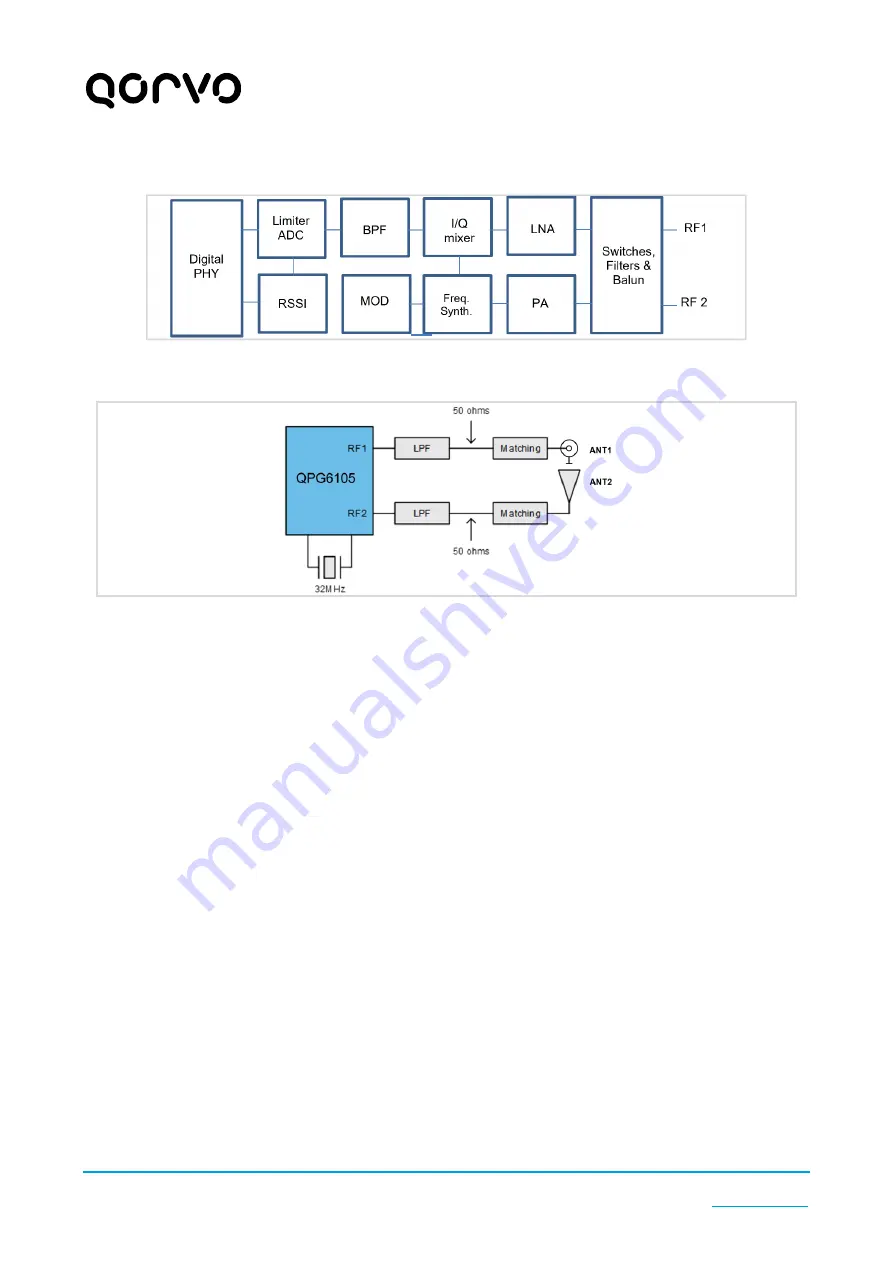
Figure 1: RF Block Diagram of the QPG6105 Chip 


Figure 2: RF Block Diagram of the QPE6105A Module with one Embedded Antenna and  

one Antenna Pin 


2.1 

General Description


The  QPG6105  chip  is  an 

IEEE  802.15.4  /  Bluetooth


Low  Energy 

Multi-Protocol  Multi-Channel 

Communications Controller for ultra-low power wireless. It is compliant with the IEEE Standard 802.15.4 for 
Zigbee, and the Bluetooth Core Specification version 5.3 for Bluetooth Low Energy. 

2.2 

Power Regulation


The QPG6105  chip has an integrated power management system  using  a Global  Low Dropout Regulator 
(GLDO).  This  generates  an  internal  1.8 V  power  supply.  The  internal  1.8 V  power  rail  is  used  to  supply 
separate  local  LDO  regulators  feeding  RF/analog  and  digital  blocks.  The  local  LDOs  used  to  supply 
RF/analog blocks are specially designed to have high power supply rejection ratio (PSRR) to suppress the 
supply ripples.  

In case the external supply voltage is too low to deliver the 1.8V internal supply voltage, the QPG6105 chip 
will reset and consequently stop all RF communication. This means that RF frequency and RF modulation 
will be independent from the supply voltage.  

2.3 

Frequency Synthesis and Modulation


The QPG6105 chip uses a FLL circuit with a VCO operating at 2 times of the transmit frequency. The VCO 
is  directly  modulated  by  a  Digital  Signal  Processor  (DSP).  The  modulation  is  fully  compatible  with  Offset 
Quadrature Phase-Shift Keying (O-QPSK) and MSK modulation as used by Bluetooth Low Energy. 

The  receiver  uses  a  low  Intermediate  Frequency  (IF)  scheme,  where  the  IF  frequency  is  2  MHz. 
The formula to calculate the VCO frequency in RX mode can be found in section 3.6.2. 

2.4 

RF Interface 

The QPE6105A module has two RF outputs: RF1 and RF2. Both RF ports are bidirectional and will be used 
for both transmit (TX) and receive (RX) mode. The antenna ports outputs are 50 

Ω single ended. Only one 

antenna  is  used  for  RX  or  TX  at  the  time  (i.e.,  not  supporting  MIMO).  Antenna  Diversity  is  supported  in 

Summary of Contents for QPE6105A

Page 1: ...Information 4 3 1 Applicable Standard 4 3 2 Duty Cycle Correction Spurious Emission According Section 15 35 c 4 3 3 Bluetooth Low Energy Duty Cycle Correction Factor 5 3 3 1 Application limited 5 3 3...

Page 2: ...ts reserved 2022 2023 Qorvo Inc GP335_UM_20021 Version 1 00 Page 2 of 15 www qorvo com 1 Device under Test DUT This certification guide has been customized for the following product Type QPE6105A Mode...

Page 3: ...F analog blocks are specially designed to have high power supply rejection ratio PSRR to suppress the supply ripples In case the external supply voltage is too low to deliver the 1 8V internal supply...

Page 4: ...r than 0 1 seconds or in cases where the pulse train exceeds 0 1 seconds the measured field strength shall be determined from the average absolute voltage during a 0 1 second interval during which the...

Page 5: ...Summary FCC Duty Cycle Correction IF connection interval is 50 ms the frequency spreading provides 6 dB duty cycle correction The maximum duty cycle in Application Mode combined with the frequency dom...

Page 6: ...on mobile devices CFR 47 Part 1 1 1310 Radiofrequency radiation exposure limits The DUT is classified as a mobile device so the applicable distance for the radiation exposure evaluation is 20 cm 0 2 m...

Page 7: ...nsist of a Radio Control Console RCC PC application and Product Test Component PTC firmware binaries Below figure shows the high level overview of the system Figure 3 System Setup The physical interfa...

Page 8: ...cation Guide Bluetooth Low Energy Mode Subject to change without notice All rights reserved 2022 2023 Qorvo Inc GP335_UM_20021 Version 1 00 Page 8 of 15 www qorvo com Figure 5 Pinning of the QPE6105a...

Page 9: ...re 6 Connecting Power Supply and UART Interface on Radio Adaptor Board Connecting power supply and UART interface on adaptor board Commands Descriptions JP1 UFL connector for ANT_RF1 J1 pin 1 39 GND J...

Page 10: ...mmands PHY BLE RF4CE Select the BLE or RF4CE Zigbee PHY I Print display the current settings state of the chip AN 0 Select antenna port 0 CH 20 Set channel to channel 20 channel 0 to 39 can be selecte...

Page 11: ...0x008e 0x007 It is recommended to copy paste the command in the Console window To verify if the correct data is written the following command can be used RR 0x008e will display content of register 0x...

Page 12: ...in transmission order 2 repeated 10101010 in transmission order 3 PRBS15 sequence 4 repeated 11111111 in transmission order sequence 5 repeated 00000000 in transmission order sequence 6 repeated 0000...

Page 13: ...dio Control Console application 5 5 1 Select RF Channel See section 5 3 3 an RF channel 5 5 2 Turn RX On Make sure TX is OFF RX ON switch receiver ON 5 5 3 Print Packets Sent Received in BLE Mode RX O...

Page 14: ...11 Electronic Code of Federal Regulations e CFR Title 47 Part 15 Radio Frequency Devices 12 FCC Publication number 558074 D01 15 247 Meas Guidance v05r02 pdf 13 ANSI C63 10 2013 Procedures for Compli...

Page 15: ...ED HEREIN AND QORVO HEREBY DISCLAIMS ANY AND ALL WARRANTIES WITH RESPECT TO SUCH PRODUCTS WHETHER EXPRESS OR IMPLIED BY LAW COURSE OF DEALING COURSE OF PERFORMANCE USAGE OF TRADE OR OTHERWISE INCLUDIN...

Reviews: