background image

MITX-V1K0 Series - User Guide, Rev. 1.0 


www.quanmax.com 


// 81 


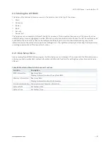
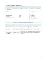
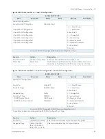
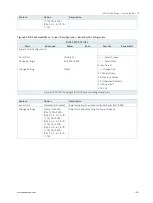
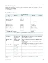
Feature 

Option 

Description 

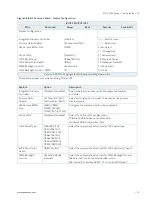
11, 12;], [IO=2F8h; 
IRQ=3, 4, 5, 6, 7, 9, 10, 
11, 12;], [IO=3E8h; 
IRQ=3, 4, 5, 6, 7, 9, 10, 
11, 12;], [IO=2E8h; 
IRQ=3, 4, 5, 6, 7, 9, 10, 
11, 12;] 

Serial Port 1 Type 

[RS232], [RS422], 
[RS485] 

Select an appropriate type for Serial Port 1. 

RS485 Duplex Mode 

[Half Duplex], [Full 
Duplex] 

Select an appropriate RS485 Duplex Mode. 

RS485 Auto Flow 
Control 

[Disabled], [Enabled] 

Select whether to enable or disable RS485 Auto Flow Control. 


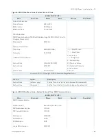
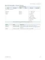
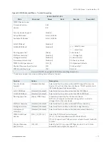
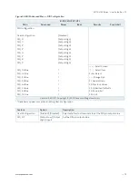
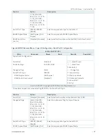
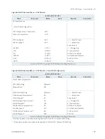
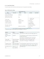
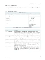
Figure 58: BIOS Advanced Menu - Super IO Configuration - Serial Port 2 Configuration 

BIOS SETUP UTILITY 

Main 

Advanced 

Power 

Boot 

Security 

Save & Exit 

Super Port 2 Configuration 


Serial Port 

[Enabled] 


: Select Screen 

Device Settings 

IO=2F8h; IRQ=3; 


: Select Item 


Enter: Select 

Change Setting 

[Auto] 

+/-: Change Opt. 

Serial Port 2 Type 

[RS232] 

F1: General Help 

RS485 Deplux Mode* 

[Half Duplex] 

F2: Previous Values 

RS485 Auto Flow Control* 

[Disabled] 

F3: Optimized Defaults 


F4: Save & Exit 


ESC: Exit 

Version 2.20.1271. Copyright (C) 2019, American Megatrends, Inc. 

* These items appear only when selecting RS485 for the Serial Port 2 Type. 


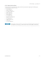
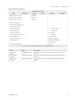
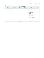
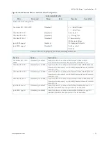
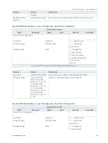
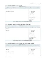
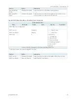
Feature 

Option 

Description 

Serial Port 

[Disabled], [Enabled] 

Select whether to enable or disable Serial Port (COM). 

Change Settings 

[Auto], [IO=2F8h; 
IRQ=3;], [IO=3F8h; 
IRQ=3, 4, 5, 6, 7, 9, 10, 
11, 12;], [IO=2F8h; 
IRQ=3, 4, 5, 6, 7, 9, 10, 
11, 12;], [IO=3E8h; 
IRQ=3, 4, 5, 6, 7, 9, 10, 
11, 12;], [IO=2E8h; 
IRQ=3, 4, 5, 6, 7, 9, 10, 
11, 12;] 

Select an optional setting for Super IO device. 

Serial Port 2 Type 

[RS232], [RS422], 
[RS485] 

Select an appropriate type for Serial Port 2. 

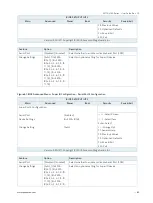
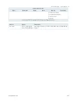
RS485 Duplex Mode 

[Half Duplex], [Full 

Select an appropriate RS485 Duplex Mode. 

Summary of Contents for MITX-V1K0 Series

Page 1: ...USER GUIDE www quanmax com MITX V1K0 Series Doc User Guide Rev 1 0 Doc ID To be Determined...

Page 2: ...MITX V1K0 Series User Guide Rev 1 0 www quanmax com 2 This page has been intentionally left blank...

Page 3: ...be suitable for the specified use without further testing or modification Quanmax expressly informs the user that this user guide only contains a general description of processes and instructions whic...

Page 4: ...rely at your risk To minimize the risks associated with your products and applications you should provide adequate design and operating safeguards You are solely responsible for compliance with all le...

Page 5: ...or visit our website Customer Support Find Quanmax contacts by visiting our website Customer Service As a trusted technology innovator and global solutions provider Quanmax extends its embedded market...

Page 6: ...rescribed by the law may endanger your life health and or result in damage to your material ESD Sensitive Device This symbol and title inform that the electronic boards and their components are sensit...

Page 7: ...es before performing any work on this product Earth ground connection to vehicle s chassis or a central grounding point shall remain connected The earth ground cable shall be the last cable to be disc...

Page 8: ...If it is necessary to store or ship the product then re pack it in the same manner as it was delivered Special care is necessary when handling or unpacking the product See Special Handling and Unpacki...

Page 9: ...fications 20 3 5 Processor Support 21 3 6 System Memory Support 21 3 6 1 Memory Operating Frequencies 21 3 7 On board Graphics Subsystem 22 3 8 Power Supply Voltage 22 4 Connector Locations 24 4 1 Top...

Page 10: ...LVDE_EDID Selection JP9 65 8 BIOS 66 8 1 Starting the uEFI BIOS 66 8 2 Starting the uEFI BIOS 67 8 2 1 Main Setup Menu 67 8 2 2 Advanced Setup Menu 70 8 2 3 Power Setup Menu 89 8 2 4 Boot Setup Menu...

Page 11: ...E2 56 Table 42 Pin Assignment PCIE1 59 Table 43 Pin Assignment CN13 CN14 61 Table 44 Pin Assignment JP1 JP2 62 Table 45 Pin Assignment JP4 63 Table 46 Pin Assignment JP4 63 Table 47 Pin Assignment JP6...

Page 12: ...D Firmware Version 68 Figure 47 BIOS Advanced Menu 71 Figure 48 BIOS Advanced Menu Display Configuration 72 Figure 49 BIOS Advanced Menu CPU Chipset Configuration 73 Figure 50 BIOS Advanced Menu NVMe...

Page 13: ...MITX V1K0 Series User Guide Rev 1 0 www quanmax com 13...

Page 14: ...MITX V1K0 Series board s special features and is not intended to be a standard PC AT textbook New users are recommended to study the short installation procedure stated in the following chapter befor...

Page 15: ...rwise components RAM LAN cards etc might get damaged Make sure to use a standard ATX12V PSU with suitable cable kits and PS ON active 2 Insert the DDR4 SO DIMM 260 pin module s Be careful to push the...

Page 16: ...ble rating to withstand the maximum available power The peripheral device enclosure fulfils the IEC60950 1 fire protecting requirements 2 3 Lithium Battery Replacement If replacing the lithium battery...

Page 17: ...nstruksjoner VARNING Explosionsfara vid felaktigt batteribyte Anv nd samma batterityp eller en ekvivalent typ som rekommenderas av apparattillverkaren Kassera anv nt batteri enligt fabrikantens instru...

Page 18: ...MITX V1K0 Series User Guide Rev 1 0 www quanmax com 18 3 System Specifications 3 1 System Block Diagram Figure 1 System Block Diagram MITX V1K0 Series...

Page 19: ...x by header 2x S PDIF 1x on rear 1x by header Network Connection Ethernet 3x GbE LAN RJ45 on rear 2x Intel I211 AT 1x Intel I210 AT Peripheral Connection USB 2x USB 3 1 Type A on rear 5x USB 2 0 2x Ty...

Page 20: ...Support Windows 10 Mechanical Dimension L x W Mini ITX 170 mm x 170 mm 6 70 x 6 70 3 3 Environmental Conditions The MITX V1K0 Series is compliant with the following environmental conditions It is the...

Page 21: ...re and the actual worst case load of processor 3 6 System Memory Support The MITX V1K0 Series has two DDR4 SO DIMM sockets The sockets support the following memory features 2x DDR4 SO DIMM 1 2 V Up to...

Page 22: ...ll MITX V1K0 Series versions support four displays pipes Up to four displays can be used simultaneously and be used to implement independent or cloned display configuration Table 6 Four displays Confi...

Page 23: ...r Guide Rev 1 0 www quanmax com 23 The requirements to the voltages of ATX power supply are as follows Table 7 Supply Voltages Supply Min Max Note 12 V 11 4 V 12 6 V Should be 5 for compliance with th...

Page 24: ...per List Item Designation Description See Chapter 1 JP1 Pin 9 Selection for COM1 7 20 1 2 JP2 Pin 9 Selection for COM2 7 20 1 3 JP3 AT ATX Power Mode Selection 7 20 2 4 JP4 USB Power Selection 7 20 3...

Page 25: ...ity LED Pin Header 7 19 22 CN14 M 2 Key B LED Pin Header 7 19 23 CN15 S PDIF Output Pin Header 7 9 24 CN19 Right Channel 3W Audio AMP Output Wafer 7 6 25 CN23 Panel Backlight Wafer for LVDS1 7 12 26 C...

Page 26: ...Panel 2 Pin Header 7 8 4 2 Bottom Side Figure 3 Bottom Side Table 10 Bottom Side Internal Connector Pin Assignment Item Designation Description See Chapter 1 M2M1 M 2 Key M Socket for SATA1 BOM optio...

Page 27: ...ee Chapter 1 CN16 GbE LAN2 GbE LAN3 Connector 6 2 2 CN17 GbE LAN1 USB 3 1 Port 0 1 Connector 6 2 6 3 3 CN18 3 Stack up Azalia Audio Phone Jack 6 4 4 CN20B Single DisplayPort Connector Configuration 1...

Page 28: ...the pin numbers in the connector Signal The abbreviated name of the signal at the current pin The notation XX states that the signal XX is active low Note Special remarks concerning the signal Designa...

Page 29: ...scription Note 1 TX0 DisplayPort Lane 0 transmitter differential pair 2 GND Ground 3 TX0 DisplayPort Lane 0 transmitter differential pair 4 TX1 DisplayPort Lane 1 transmitter differential pair 5 GND G...

Page 30: ...s the first pair in 1000Base T i e the BI_DA pair and is the transmit pair in 10Base T and 100Base TX In MDI crossover mode this pair acts as the BI_DB pair and is the receive pair in 10Base T and 100...

Page 31: ...B device 2 USB_D USB 2 0 differential pair 3 USB_D USB 2 0 differential pair 4 GND Ground Figure 8 USB 3 1 Connector CN17 USB 3 1 Port 0 1 Table 15 Pin Assignment USB 3 1 Connector CN17 USB 3 1 Port 0...

Page 32: ...se only HiSpeed USB cable specified in USB3 0 standard Figure 10 USB 3 0 High Speed Cable On Twisted Power Pair Red Vbus Black Power Ground Inner Shield Aluminum Metallized Polyester 28 AWG Tinned Cop...

Page 33: ...speaker connectors CN19 CN25 Figure 11 Audio Jack CN18 Table 16 Pin Assignment Audio Jack CN18 Pin Signal Description Note Top Tip Line In_L Audio input left channel signal Ring Line In_R Audio input...

Page 34: ...ing to the motherboard 7 1 1 2x4 pin ATX Power Supply Wafer ATX1 The 2x4 pin ATX power supply wafer provides 12 V DC to the board Figure 12 2x4 pin ATX Power Supply Wafer ATX1 Table 17 Pin Assignment...

Page 35: ...he connection of the FAN for the CPU while the System FAN Wafer FAN2 for the connection of the FAN for the system Figure 14 Fan Wafer FAN1 FAN2 Table 19 Pin Assignment FAN1 FAN2 Pin Signal Description...

Page 36: ...TA2 Table 20 Pin Assignment SATA1 SATA2 Pin Signal Description Note 1 GND Ground 2 TX Host transmitter differential signal pair 3 TX Host transmitter differential signal pair 4 GND Ground 5 RX Host re...

Page 37: ...ion Note 1 USBVCC 5 V supply SB5V is supplied during power down to allow wakeup 2 USBVCC 5 V supply SB5V is supplied during power down to allow wakeup 3 USB_A USB 2 0 differential pair for channel A 4...

Page 38: ...pair 4 GND Ground 7 6 Speaker Connector CN19 CN25 The Speaker audio out interface is available through the wafers CN19 and CN25 These outputs are shared with the audio output Line out signals of the a...

Page 39: ...peaker connectors CN19 CN25 Figure 21 Front Panel Audio Pin Header CN28 Table 26 Pin Assignment CN28 Pin Signal Description Note 1 MIC2 L Microphone input left channel signal 2 Audio GND Audio ground...

Page 40: ...data is ready from or written to the HDD 6 Internal Speaker Internal system warning speaker 7 HDD LED HDD activity LED 8 Speaker External system warning speaker Internal Buzzer is enabled when Pin6 8...

Page 41: ...m battery is low It also can be used to signal some other external power management event 8 SMBus Data System management bus bidirectional data line 9 GND Ground 10 SMBus Clock System management bus b...

Page 42: ...re 25 Serial COM CN3 CN4 CN5 CN7 CN8 CN10 Table 30 Pin Assignment CN3 CN4 Pin RS232 Signal RS422 Signal Half Duplex RS485 Signal Full Duplex RS485 Signal Note 1 DCD TX DATA TX 2 DSR N A N A N A 3 RXD...

Page 43: ...o the modem etc that the on board UART is ready to establish communication link DSR Data Set Ready indicates that the modem etc is ready to establish a communications link RTS Request To Send indicate...

Page 44: ...l pair 8 TxclkB LVDS Channel B clock differential pair 9 GND Ground 10 GND Ground 11 TxoutA0 LVDS Channel A Data 0 differential pair 12 TxoutB0 LVDS Channel B Data 0 differential pair 13 TxoutA0 LVDS...

Page 45: ...l A Data 3 differential pair 24 TxoutB3 LVDS Channel B Data 3 differential pair 25 TxoutA3 LVDS Channel A Data 3 differential pair 26 TxoutB3 LVDS Channel B Data 3 differential pair 27 GND Ground 28 G...

Page 46: ...ght inverter Figure 27 Backlight Power Output Wafer CN23 Table 34 Pin Assignment CN23 Pin Signal Description Note 1 BL_EN Backlight Enable signal 2 BL_ADJ_PWM Backlight Adjustment PWM Pulse Width Modu...

Page 47: ...nput Output Wafer CN2 Table 35 Pin Assignment CN2 Pin Signal Description Note 1 5V 5 V power supply 2 DIO_0 Digital input output channel 0 3 DIO_1 Digital input output channel 1 4 DIO_2 Digital input...

Page 48: ...standby power supply 3 Reserved 4 Ground 5 Reserved 6 1 5V 1 5 V power supply 7 CLKREQ Reference clock request signal 8 UIM_PWR Power source for User Identity Modules UIM 9 Ground 10 UIM_DATA Data si...

Page 49: ...tter differential pair 34 Ground 35 Ground 36 USB_D USB 2 0 differential pair 37 Ground 38 USB_D USB 2 0 differential pair 39 3 3VSB 3 3 V standby power supply 40 Ground 41 3 3VSB 3 3 V standby power...

Page 50: ...makes it possible to use a WWAN wireless modem in this M 2 socket The M 2 Key M sockets M2M1 M2M2 supports SATA signals They share the same SATA signals with the SATA connectors SATA1 SATA2 respective...

Page 51: ...PCIe Lane 1 USB 3 0 transmitter differential pair 36 UIM PWR Power source for User Identity Modules UIM 37 M2B1_TXP USB3 0 TX PCIe Lane 1 USB 3 0 transmitter differential pair 38 NC 39 GND Ground 40...

Page 52: ...k supply input 69 NC 70 3 3V 3 3 V power supply 71 GND Ground 72 3 3V 3 3 V power supply 73 GND Ground 74 3 3V 3 3 V power supply 75 NC These pins are connected to SIM card connector SIM1 directly The...

Page 53: ...3 3 V power supply 17 NC 18 3 3V 3 3 V power supply 19 NC 20 NC 21 GND Ground 22 NC 23 NC 24 NC 25 NC 26 NC 27 GND Ground 28 NC 29 NC 30 NC 31 NC 32 NC 33 GND Ground 34 NC 35 NC 36 NC 37 NC 38 DEVSLP...

Page 54: ...ifferential pair 50 NC 51 GND Ground 52 NC 53 NC 54 NC 55 NC 56 NC 57 GND Ground 58 NC 59 KEY M 60 KEY M 61 KEY M 62 KEY M 63 KEY M 64 KEY M 65 KEY M 66 KEY M 67 NC 68 NC 69 GND Ground 70 3 3V 3 3 V p...

Page 55: ...2 Micro SIM Card Cage SIM1 Table 39 Pin Assignment SIM1 Pin Signal Description Note 1 UIM_PWR Power 5V or 3 3V 2 UIM_RESET Reset signal 3 UIM_CLK Clock signal 4 GND Ground 5 UIM_VPP Programming voltag...

Page 56: ...IE2 which supports PCIe x8 signal only Figure 34 PCIe x16 Slot Connector PCIE2 Table 41 Pin Assignment PCIE2 Pin Side B Side A Signal Description Signal Description 1 12V 12 V power PRSNT1 Hot plug pr...

Page 57: ...nsmitter differential pair Ground 25 Ground HSIP2 Lane 2 receiver differential pair 26 Ground HSIN2 Lane 2 receiver differential pair 27 HSOP3 Lane 3 transmitter differential pair Ground 28 HSON3 Lane...

Page 58: ...C Reserved 51 NC Ground 52 Ground NC 53 Ground NC 54 NC Ground 55 NC Ground 56 Ground NC 57 Ground NC 58 NC Ground 59 NC Ground 60 Ground NC 61 Ground NC 62 NC Ground 63 NC Ground 64 Ground NC 65 Grou...

Page 59: ...Table 42 Pin Assignment PCIE1 Pin Side B Side A Signal Description Signal Description 1 12V 12 V power PRSNT1 Hot plug presence detect 2 12V 12 V power 12V 12 V power 3 NC 12V 12 V power 4 Ground Gro...

Page 60: ...RSNT2 1 Hot plug presence detect PERX0 Lane 0 receiver differential pair 18 Ground Ground 19 PETX1 Lane 1 transmitter differential pair NC 20 PETX1 Lane 1 transmitter differential pair Ground 21 Groun...

Page 61: ...eader CN13 CN14 The pin header CN13 is intended to connect mPCIe activity LED cable The pin header CN14 is intended to connect M 2 Key B activity LED cable Figure 36 mPCIe M 2 Key B LED Pin Header CN1...

Page 62: ...one of the lines surrounding a jumper pin is thick which indicates pin No 1 To move a jumper from one position to another use needle nose pliers or tweezers to pull the pin cap off the pins and move...

Page 63: ...Selection JP4 The USB Power Selection jumper JP4 can be used to determine whether the USB ports are powered in the S4 S5 state Figure 40 USB Power Selection JP4 Table 46 Pin Assignment JP4 Jumper Pos...

Page 64: ...wer is disconnected the battery will fully deplete within a few weeks 7 20 5 Backlight Power Enable Selection for LVDS1 JP7 The jumper JP7 can be used to select voltage level of backlight enable signa...

Page 65: ...ssignment JP8 Jumper 1 Position Description Pin 1 3 Pin 3 5 X Backlight Power 12 V X Backlight Power 5 V Jumper 2 Position Description Pin 2 4 Pin 4 6 X Panel Power 3 3 V X Panel Power 5 V X Jumper se...

Page 66: ...BIOS is password protected a request for password will appear Enter either the User Password or the Supervisor Password see Security menu press RETURN and proceed with step 5 5 A setup menu will appea...

Page 67: ...rmation about the status or the operational configuration The right frame displays an Item Specific Help window providing an explanation of the respective function 8 2 1 Main Setup Menu Upon entering...

Page 68: ...eral Help System Date Mon 09 23 2019 F2 Previous Values System Time 21 51 51 F3 Optimized Defaults F4 Save Exit Access Level Administrator ESC Exit Version 2 20 1271 Copyright C 2019 American Megatren...

Page 69: ...D MP2 FW Version 1 0 24 Select Screen Select Item XHCI FW Version FF FF FF FF Enter Select VBIOS FW Version 0113 Change Opt GOP Driver Version 0 F1 General Help F2 Previous Values EC FW Version 0CFF F...

Page 70: ...ing sub screen functions are included in the menu LAN Configuration Display Configuration CPU Chipset Configuration NVMe Configuration SATA Configuration USB Configuration Trusted Computing Network St...

Page 71: ...work Stack Configuration Change Opt DIO Configuration F1 General Help Super IO Configuration F2 Previous Values H W Monitor F3 Optimized Defaults F4 Save Exit Tls Auth Configuration ESC Exit Version 2...

Page 72: ...cs Controller Disabled Enabled Select whether to enable or disable Integrated Graphics controller Primary Video Adaptor Int Graphics IGD Ext Graphics PEG Select which graphic controller to be used as...

Page 73: ...Item IOMMU Enabled Enter Select Change Opt F1 General Help F2 Previous Values F3 Optimized Defaults F4 Save Exit ESC Exit Version 2 20 1271 Copyright C 2019 American Megatrends Inc Feature Option Des...

Page 74: ...ation BIOS SETUP UTILITY Main Advanced Power Boot Security Save Exit NVMe Configuration No NVMe Device Found Select Screen Select Item Enter Select Change Opt F1 General Help F2 Previous Values F3 Opt...

Page 75: ...A Controller Enabled Select Screen Select Item Serial ATA Port 0 Not Present Enter Select Serial ATA Port 1 Not Present Change Opt F1 General Help F2 Previous Values F3 Optimized Defaults F4 Save Exit...

Page 76: ...ults F4 Save Exit ESC Exit Version 2 20 1271 Copyright C 2019 American Megatrends Inc Feature Option Description Legacy USB Support Enabled Disabled Auto Select whether to enable or disable Legacy USB...

Page 77: ...to enable or disable BIOS support for security device O S will not show Security Device TCG EFI protocol and INT1A interface will not be available SHA 1 PCR Bank Disabled Enabled Select whether to ena...

Page 78: ...oard UNDI Universal Network Driver Interface for Intel I211 I210 LAN Boot I211 AT 1 Disabled Load PXE Select whether to enable or disable load onboard PXE Preboot Execution Environment or uEFI SNP Sim...

Page 79: ...igh Select Screen DIO_0 Value 1 Select Item DIO_1 Value 1 Enter Select DIO_2 Value 1 Change Opt DIO_3 Value 1 F1 General Help DIO_4 Value 1 F2 Previous Values DIO_5 Value 1 F3 Optimized Defaults DIO_6...

Page 80: ...No Protection UART device have be entry D3 for OS control Keep Device On Protection UART device not entry D3 state Figure 57 BIOS Advanced Menu Super IO Configuration Serial Port 1 Configuration BIOS...

Page 81: ...ice Settings IO 2F8h IRQ 3 Select Item Enter Select Change Setting Auto Change Opt Serial Port 2 Type RS232 F1 General Help RS485 Deplux Mode Half Duplex F2 Previous Values RS485 Auto Flow Control Dis...

Page 82: ...ized Defaults F4 Save Exit ESC Exit Version 2 20 1271 Copyright C 2019 American Megatrends Inc Feature Option Description Serial Port Disabled Enabled Select whether to enable or disable Serial Port C...

Page 83: ...tting for Super IO device Figure 61 BIOS Advanced Menu Super IO Configuration Serial Port 5 Configuration BIOS SETUP UTILITY Main Advanced Power Boot Security Save Exit Super Port 5 Configuration Seri...

Page 84: ...tings IO 2E0h IRQ 5 Select Item Enter Select Change Setting Auto Change Opt F1 General Help F2 Previous Values F3 Optimized Defaults F4 Save Exit ESC Exit Version 2 20 1271 Copyright C 2019 American M...

Page 85: ...nds Inc Figure 64 BIOS Advanced Menu H W Monitor Smart FAN Configuration BIOS SETUP UTILITY Main Advanced Power Boot Security Save Exit Smart FAN Configuration CPU FAN Setting Manual Manual Duty 255 S...

Page 86: ...0 Series User Guide Rev 1 0 www quanmax com 86 Feature Option Description CPU FAN Setting Manual Smart Select CPU smart FAN configuration System FAN Setting Manual Smart Select system smart FAN config...

Page 87: ...ed Menu Tls Auth Configuration Server CA Configuration BIOS SETUP UTILITY Main Advanced Power Boot Security Save Exit Enroll Cert Delete Cert Select Screen Select Item Enter Select Change Opt F1 Gener...

Page 88: ...er Boot Security Save Exit F2 Previous Values F3 Optimized Defaults F4 Save Exit ESC Exit Version 2 20 1271 Copyright C 2019 American Megatrends Inc Feature Option Description Cert GUID 11111111 2222...

Page 89: ...it Version 2 20 1271 Copyright C 2019 American Megatrends Inc Feature Option Description ACPI Sleep State Suspend Disabled S3 Suspend to RAM Select the highest ACPI sleep state the system will enter w...

Page 90: ...ration BIOS SETUP UTILITY Main Advanced Power Boot Security Save Exit WatchDog Timer Configuration WDT Function Disabled Select Screen WDT Count Mode Minute Select Item WDT Timer 3 Enter Select Change...

Page 91: ...Inc These items appear only when selecting UEFI and Legacy or UEFI only Feature Option Description Full Screen LOGO Display Disabled Enabled Select whether to enable or disable to display logo screen...

Page 92: ...the User s password is set then this is a power on password and must be entered to boot or enter Setup In Setup the User will have Administrator rights The password length must be in the following ra...

Page 93: ...record of all passwords in a safe place Forgotten passwords results in being locked out of the system If the system cannot be booted because the User Password or the Supervisor Password are not know c...

Page 94: ...lect this option a confirmation window appears Select Yes to save changes and exit Discard Changes and Exit Exit system setup without saving any changes Select this option only if you do not want to s...

Page 95: ...Drive HDMI High Definition Multimedia Interface LAN Local Area Network LED Light Emitting Device LVDS Low Voltage Differential Signaling ME F W Management Engine Firmware mPCIe mini Peripheral Compon...

Page 96: ...acilities for individual users and business firms in all industries including but not limited to the following four categories Infotainment Automation IoT and Network Communications on the basis of di...

Reviews: