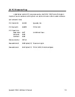
14 FIFO Control Register
The FIFO Control Register is used to control the internal data FIFOs. The
address of this register is Base+A (hex). Table 13 details the bit definitions of the
register. This register can be ignored if the internal FIFOs are not being used.
TX_RESET
0
0
0
RX_RESET
EN_TO
EN_PAT
0
Bit 0
Bit 1
Bit 2
Bit 3
Bit 4
Bit 5
Bit 6
Bit 7
Table 13 --- FIFO Control Register - Read/Write
Bit 7:
Reserved, always 0.
Bit 6:
EN_PAT --- Enable Receive Pattern Detection:
Set
this bit (logic 1), to enable the receive pattern detection circuitry. Clear
this bit (logic 0), to disable pattern detection. See page 37 for details on
the receive pattern detection feature.
Bit 5:
EN_TO --- Enable Receive Timeout:
Set this bit (logic 1), to enable the internal receive FIFO timeout. Clear this
bit (logic 0), to disable the receive FIFO timeout. See page 38 for details
on the receive FIFO timeout feature.
Bit 4:
RX_RESET --- Reset Receive FIFO
:
Set (logic 1), then clear (logic 0) this bit to reset the internal receive FIFO.
The FIFO can be reset only when it is disabled.
Bits 3-1:
Reserved, always 0.
Bit 0:
TX_RESET --- Reset Transmit FIFO
:
Set (logic 1), then clear (logic 0) this bit to reset the internal transmit FIFO.
The FIFO can be reset only when it is disabled.
Quatech MPAC-100 User's Manual
42


