background image


                                           SC200L Hardware Design


 SC200L_Hardware_Design

                                                      10 / 103 


3


Application Interfaces 


3.1. General Description 

 
SC200L is an SMD type module with 146 LCC pins and 128 LGA pins. The following chapters provide the 
detailed description of pins/interfaces listed below.   


 Power 

supply 

 USB 

interface 

 UART 

interfaces 

 (U)SIM 

interfaces 

 GPIO 

interfaces 

 I2C 

interface 

 SPI 

interfaces 

 ADC 

interfaces


 LCM 

interfaces


 Touch 

panel 

interface 

 Camera 

interfaces 

 Sensor 

interfaces 

 Audio 

interfaces 

 Emergency 

download 

interface 


Summary of Contents for 2021SC200LEM

Page 1: ...SC200L EM Hardware Design Smart module series Rev 1 0 Date 2020 9 21 Status Controlled Documents www quectel com ...

Page 2: ...MATION PROVIDED IS BASED UPON CUSTOMERS REQUIREMENTS QUECTEL MAKES EVERY EFFORT TO ENSURE THE QUALITY OF THE INFORMATION IT MAKES AVAILABLE QUECTEL DOES NOT MAKE ANY WARRANTY AS TO THE INFORMATION CONTAINED HEREIN AND DOES NOT ACCEPT ANY LIABILITY FOR ANY INJURY LOSS OR DAMAGE OF ANY KIND INCURRED BY USE OF OR RELIANCE UPON THE INFORMATION ALL INFORMATION SUPPLIED HEREIN IS SUBJECT TO CHANGE WITHO...

Page 3: ...SC200L Hardware Design SC200L_Hardware_Design 3 103 About the Document Revision History Revision Date Author Description 1 0 2020 9 21 Jeffrey Andy Initial ...

Page 4: ...Using the PWRKEY 26 3 5 2 Turn off Module 28 3 6 Power Output 28 3 7 Battery Charge and Management 29 3 8 USB Interface 30 3 9 UART Interfaces 33 3 10 U SIM Interface 34 3 11 SD Card Interface 36 3 12 GPIO Interfaces 38 3 13 I2C Interfaces 40 3 14 SPI Interfaces 40 3 15 ADC Interface 41 3 16 LCM Interface 42 3 17 Touch Panel Interface 44 3 18 Camera Interface 45 3 19 Sensor Interfaces 49 3 20 Audi...

Page 5: ...nstallation 67 6 4 1 Antenna Requirements 67 6 4 2 Recommended RF Connector for Antenna Installation 68 6 Electrical Reliability and Radio Characteristics 70 7 1 Absolute Maximum Ratings 70 7 2 Power Supply Ratings 70 7 3 Operation and Storage Temperatures 71 7 4 Current Consumption 71 7 5 RF Output Power 74 7 6 RF Receiving Sensitivity 76 7 7 Electrostatic Discharge 77 7 Mechanical Dimensions 78 ...

Page 6: ...y with laws and regulations restricting the use of wireless devices while driving Switch off the cellular terminal or mobile before boarding an aircraft The operation of wireless appliances in an aircraft is forbidden to prevent interference with communication systems If the device offers an Airplane Mode then it should be enabled prior to boarding an aircraft Please consult the airline staff for ...

Page 7: ...to TV set radio computer or other electric equipment In locations with potentially explosive atmospheres obey all posted signs to turn off wireless devices such as your phone or other cellular terminals Areas with potentially explosive atmospheres include fuelling areas below decks on boats fuel or chemical transfer or storage facilities areas where the air contains chemicals or particles such as ...

Page 8: ...SS BeiDou satellite positioning systems Support multiple audio and video codecs Built in high performance Mail T820 graphics processing unit Provide multiple audio and video input output interfaces as well as abundant GPIO interfaces SC200L module is available in three variants SC200L CE SC200L EM SC200L WF Table 1 SC200L EM frequency bands Mode Frequency band LTE FDD B1 B2 B3 B5 B7 B8 B20 B28 LTE...

Page 9: ...To help customers design and test applications with Quectel SC200L modules Quectel supplies an evaluation kit which includes an evaluation board a USB to RS232 converter cable a USB T data cable a power adapter an earphone and antennas For details please refer the document 1 ...

Page 10: ...ins and 128 LGA pins The following chapters provide the detailed description of pins interfaces listed below Power supply USB interface UART interfaces U SIM interfaces GPIO interfaces I2C interface SPI interfaces ADC interfaces LCM interfaces Touch panel interface Camera interfaces Sensor interfaces Audio interfaces Emergency download interface ...

Page 11: ...SC200L Hardware Design SC200L_Hardware_Design 11 103 3 2 Pin Assignment The following figure shows the pin assignment of SC200Lmodule Figure 1 Pin Assignment Top View ...

Page 12: ... Bidirectional OD Open drain PI Power input PO Power output Power supply Pin Name Pin No I O Description DC Characteristics Comment VBAT_BB 1 2 PI P O Power supply for module s baseband part Vmax 4 2V Vmin 3 55V Vnorm 3 8V It must be provided with sufficient current up to 3 0A It is suggested to use a TVS for external circuit VBAT_RF 145 146 PI Power supply for module s RF part Vmax 4 20 V Vmin 3 ...

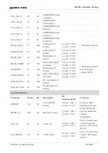
Page 13: ...7 188 189 190 191 202 203 204 206 207 208 209 210 211 212 213 214 215 216 217 218 219 220 221 222 223 224 226 227 228 229 230 231 233 234 235 236 237 238 240 241 243 244 245 247 248 250 251 255 256 258 259 261 266 268 269 271 272 273 274 Audio Interfaces Pin Name Pin No I O Description DC Characteristics Comment MIC1_P 4 AI Microphone input for channel 1 MIC1_N 5 AI Microphone input for channel 1 ...

Page 14: ... 80 V USB Interface Pin Name Pin No I O Description DC Characteristics Comment USB_VBUS 141 142 PI USB power supply Vmax 9 2V Vmin 4 5V Vnorm 5 00V Used for USB 5V power input and USB detection USB_DM 13 AI A O USB differential data bus USB 2 0 standard compliant 90Ω differential impedance USB_DP 14 AI A O USB differential data bus USB_ID 16 DI USB ID detection of the input High level by default U...

Page 15: ...annot be multiplexed into a Generic GPIOs USIM2_VDD 21 PO U SIM2 card power supply 1 80 V U SIM Vmax 1 85 V Vmin 1 75 V 2 95 V U SIM Vmax 3 1 V Vmin 2 90 V Either 1 8V or 2 95V U SIM card is supported USIM1_DET 22 DI U SIM1 card plug detection VILmax 0 48 V VIHmin 1 39 V Active low If it is not used keep it open This function is turned on by default It can be used as ordinary GPIO USIM1_RST 23 DO ...

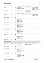
Page 16: ... 85V power domain If it is not used keep it open UART0_RXD 35 DI UART0 receive data VILmax 0 48 V VIHmin 1 39 V UART0_CTS 36 DI UART0 clear to send VILmax 0 48 V VIHmin 1 39 V UART0_RTS 37 DO UART0 request to send VOLmax 0 20 V VOHmin 1 46 V DBG_RXD 93 DI UART1 receive data Debug port by default VILmax 0 48 V VIHmin 1 39 V DBG_TXD 94 DO UART1 transmit data Debug port by default VOLmax 0 20 V VOHmi...

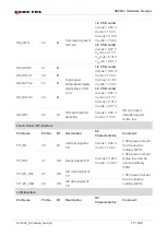
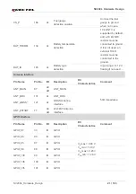
Page 17: ...O SD_DATA2 43 IO SD_DATA3 44 IO SD_DET 45 DI SD card insertion detection VILmax 0 48 V VIHmin 1 39 V SD card insert detection signal Active low Touch Panel TP Interface Pin Name Pin No I O Description DC Characteristics Comment TP_INT 30 DI Interrupt signal of TP VILmax 0 48 V VIHmin 1 39 V 1 85V power domain Can be used as ordinary GPIO TP_RST 31 DO Reset signal of TP VOLmax 0 20 V VOHmin 1 46 V ...

Page 18: ...ignal DSI_CLK_P 53 AO MIPI DSI clock signal DSI_LN0_N 54 AO MIPI DSI data 0 signal DSI_LN0_P 55 AO MIPI DSI data 0 signal DSI_LN1_N 56 AO MIPI DSI data 1 signal DSI_LN1_P 57 AO MIPI DSI data 1 signal DSI_LN2_N 58 AO MIPI DSI data 2 signal DSI_LN2_P 59 AO MIPI DSI data 2 signal DSI_LN3_N 60 AO MIPI DSI data 3 signal DSI_LN3_P 61 AO MIPI DSI data 3 signal Camera Interfaces Pin Name Pin No I O Descri...

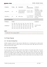
Page 19: ...VOLmax 0 20 V VOHmin 1 46 V SCAM_RST 81 DO Reset signal of camera VOLmax 0 20 V VOHmin 1 46 V SCAM_PWDN 82 DO Power down signal of camera VOLmax 0 20 V VOHmin 1 46 V CAM_I2C_SCL 83 OD I2C clock signal of camera CAM_I2C_SDA 84 OD I2C data signal of camera Keypad Interfaces Pin Name Pin No I O Description DC Characteristics Comment PWRKEY 114 DI Turn on off the module VILmax 0 60 V VIHmin 1 30 V Pul...

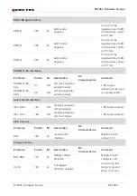
Page 20: ...OD I2C clock signal for external sensor 1 85V power domain Can be used as ordinary GPIO SENSOR_I2C_ SDA 92 OD I2C data signal for external sensor Universal I2C interface I2C4_SDA 167 OD General peripheral I2C data signal 1 85V power domain I2C4_SCL 168 OD General peripheral I2C clock signal 1 85V power domain ADC interface Pin Name Pin No I O Description DC Characteristics Comment ADC 128 AI Gener...

Page 21: ...5 AI Battery type detection Input range 0 1 2 V floating if not used Antenna interface Pin Name Pin No I O Description DC Characteristics Comment ANT_MAIN 87 AI AO ANT_MAIN 50Ω impedance ANT_DRX 131 AI ANT_DRX ANT_GNSS 1 121 AI GNSS Antenna interface ANT_WIFI BT 77 AI AO Wi Fi BT Antenna interface GPIO interface Pin Name Pin No I O Description DC Characteristics Comment GPIO_87 33 IO GPIO VILmax 0...

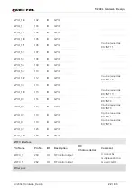
Page 22: ...ed as EXTINT12 GPIO_33 113 IO GPIO GPIO_130 115 IO GPIO Can be reused as EXTINT13 GPIO_93 116 IO GPIO Can be reused as EXTINT8 GPIO_90 117 IO GPIO Can be reused as EXTINT5 GPIO_92 118 IO GPIO Can be reused as EXTINT7 GPIO_91 119 IO GPIO Can be reused as EXTINT6 GPIO_32 123 IO GPIO GPIO_129 124 IO GPIO GRFC interface Pin Name Pin No I O Description DC Characteristics Comment GRFC_7 260 DO RF contro...

Page 23: ...nt of the module may surge up to 3A If the supply voltage is not enough there will be voltage drops and if the voltage drops below 3 1V the module will be turned off automatically Therefore please make sure the input voltage will never drop below 3 1V Pin Name Pin No I O Description DC Characteristics Comment USB_BOOT 46 DI Force the module to enter emergency download mode VILmax 0 48 V VIHmin 1 3...

Page 24: ...apacitors close to VBAT_BB RF pins The main power supply from an external application has to be a single voltage source and can be expanded to two sub paths with star structure The width of VBAT_BB trace should be no less than 3 mm In principle the longer the VBAT trace is the wider it will be In addition in order to get a stable power source it is suggested to use a TVS and place it as close to t...

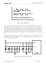
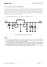
Page 25: ...put VBAT a buck converter is recommended The following figure shows a reference design for 5V input power source DC_IN C1 C2 MIC29502WU U1 IN OUT EN GND ADJ 2 4 1 3 5 VBAT 100 nF C3 470 μF C4 100 nF R2 100K 47K R3 470 μF 470R 51K R4 R1 1 1 Figure 4 Reference Circuit of Power Supply NOTES 1 It is suggested that customers should switch off the power supply for the module in an abnormal state and the...

Page 26: ... use an open drain collector driver to control the PWRKEY A simple reference circuit is illustrated in the following figure Turn on pulse PWRKEY 4 7K 47K 2 5s R1 R2 Q1 R3 1K Figure 5 Turn on the Module Using Driving Circuit The other way to control the PWRKEY is by using a button directly A TVS component is indispensable to be placed nearby the button for ESD protection A reference circuit is show...

Page 27: ...gure 7 Timing of Turning on Module NOTES 1 When the module is powered on for the first time its timing of turning on may be different from that shown above 2 Make sure that VBAT is stable before pulling down the PWRKEY pin The recommended time between them is no less than 30ms PWRKEY pin cannot be pulled down all the time ...

Page 28: ...equence diagram is as follows Figure 8 Restart timing diagram 3 6 Power Output SC200L supports the output of regulated voltages for peripheral circuits During application it is recommended to use parallel capacitors 33pF and 10pF in the circuit to suppress high frequency noise Table 6 Power Description Pin Name Default Voltage V Driving Current mA IDLE LDO1_1V85 1 85 100 KEEP LDO2_1V8 1 80 500 LDO...

Page 29: ...V mode and the charging current will decrease gradually When the battery level reaches 100 the charging is completed Table 7 Description of charging interface SC200L module supports battery temperature detection in the condition that the battery integrates a thermistor 47KΩ 1 NTC thermistor with a B constant of 3380KΩ by default the thermistor is connected to VBAT_THERM pin If the VBAT_THERM pin i...

Page 30: ... In order to avoid this VBAT_THERM should be connected to GND via a 10KΩ resistor If VBAT_THERM is unconnected the system will be unable to detect the battery making the battery cannot be charged VBAT_SNS pin must be connected Otherwise the module will have abnormalities in voltage detection as well as an associated power on off and battery charging and discharging issues The SC200L series module ...

Page 31: ...s an external USB port if it pulls down the USB_ID pin of the module the module will enter the Host mode Figure 10 USB Interface Reference Design OTG is not Supported Pin Name Pin No I O Description Comment USB_VBUS 141 142 PI USB power supply Vmax 9 20 V Vmin 4 50 V Vnorm 5 00 V USB_DM 13 AI AO USB 2 0 differential data bus USB 2 0 standard compliant 90Ω differential impedance USB_DP 14 AI AO USB...

Page 32: ...the USB connector Pay attention to the influence of junction capacitance of ESD protection devices on USB data lines Typically the capacitance value should be less than 2pF Do not route signal traces under crystals oscillators magnetic devices and RF signal traces It is important to route the USB differential traces in inner layer with ground shielding on not only the upper and lower layers but al...

Page 33: ... is equipped with a 3 3V UART interface Figure 12 Reference Circuit with Level Translator Chip for UART5 The following figure is an example of a connection between SC200L and PC A voltage level translator and an RS 232 level translator chip are also recommended to be added between the module and PC The Pin Name Pin No I O Description Comment UART0_TXD 34 DO UART0 transmit data 1 8V power domain If...

Page 34: ...default Both 1 8V and 2 95V U SIM cards are supported and the U SIM card interfaces are powered by the internal power supply of the SC200L module Table 11 Pin Definition of U SIM Interfaces Pin Name Pin No I O Description Comment USIM2_DET 17 DI U SIM2 card plug detection Active Low If it is not used keep it open Enabled by default via software It can be multiplexed into a generic GPIO USIM2_RST 1...

Page 35: ...pin U SIM card connector USIM2_VDD 21 PO U SIM2 card power supply Either 1 8V or 2 95V U SIM card is supported USIM1_DET 22 DI U SIM1 card plug detection Active Low If it is not used keep it open Enabled by default via software It can be multiplexed into a generic GPIO USIM1_RST 23 DO U SIM1 card reset signal It cannot be multiplexed into a generic GPIO USIM1_CLK 24 DO U SIM1 card clock signal It ...

Page 36: ... from each other and shield them with ground USIM_RST also needs ground protection In order to offer good ESD protection it is recommended to add a TVS diode array with parasitic capacitance not exceeding 50pF The 22Ω resistors should be added in series between the module and U SIM card so as to suppress EMI spurious transmission and enhance ESD protection Please note that the U SIM peripheral cir...

Page 37: ... Because of the high drive current it is recommended that the trace width is 0 5 mm or above In order to ensure the stability of drive power a 4 7μF and a 33pF capacitor should be added in parallel near the SD card connector CMD CLK DATA0 DATA1 DATA2 and DATA3 are all high speed signal lines In PCB design please control the characteristic impedance of them to 50Ω and do not cross them with other t...

Page 38: ...CMD and DATA should not exceed 1 mm Table 13 SD Card Trace Length Inside the Module 3 12 GPIO Interfaces SC200L has abundant GPIO interfaces with a power domain of 1 85V The pin definition is listed below Table 14 Pin Definition of GPIO Interfaces Pin No Signal Length mm 39 SD_CLK 43 50 40 SD_CMD 42 82 41 SD_DATA0 45 92 42 SD_DATA1 46 24 43 SD_DATA2 43 97 44 SD_DATA3 45 62 Pin Name Pin No GPIO Def...

Page 39: ...IO_11 103 GPIO_11 IN PD GPIO_10 104 GPIO_10 IN PD GPIO_138 105 GPIO_138 IN PU GPIO_121 106 GPIO_121 OUT L Can be reused as EXTINT11 GPIO_52 107 GPIO_52 IN PU GPIO_53 108 GPIO_53 IN PD GPIO_54 109 GPIO_54 IN PD GPIO_55 110 GPIO_55 IN PD GPIO_122 112 GPIO_122 IN PD Can be reused as EXTINT12 GPIO_33 113 GPIO_33 IN PD GPIO_130 115 GPIO_130 IN PD Can be reused as EXTINT13 GPIO_93 116 GPIO_93 IN PD Can ...

Page 40: ...I Interfaces SC200L provides three SPI interfaces which are multiplexed from UART and GPIO interfaces These interfaces can only support the master mode SPI interfaces can be used for fingerprint recognition Pin Name Pin No I O Descripti on Comment Pin Name TP_I2C_SCL 47 OD I2C clock signal of touch panel Used for touch panel TP_I2C_SDA 48 OD I2C data signal of touch panel CAM_I2C_SCL 83 OD I2C clo...

Page 41: ...ultiplexed as SPI2_DI GPIO_55 110 DO SPI2 clock signal Multiplexed as SPI2_CLK GPIO_93 116 DO SPI0 clock signal Multiplexed as SPI0_CLK GPIO_90 117 DO SPI0 chip select signal Multiplexed as SPI0_CSN GPIO_92 118 DI SPI0 data input Multiplexed as SPI0_DI GPIO_91 119 DO SPI0 data output Multiplexed as SPI0_DO GPIO_139 99 DO SPI1 chip select signal Multiplexed as SPI1_CSN GPIO_136 100 DO SPI1 data out...

Page 42: ...put power supply for LCD VCC Vnorm 2 80 V IOmax 200 mA PWM 29 DO Adjust the backlight brightness PWM control signal 1 85 V voltage domain Can be used as ordinary GPIO LCD_RST 49 DO LCD reset signal 1 85 V voltage domain Can be used as ordinary GPIO LCD_TE 50 DI LCD tearing effect signal 1 85 V voltage domain Can be used as ordinary GPIO DSI_CLK_N 52 AO LCD MIPI clock signal DSI_CLK_P 53 AO LCD MIP...

Page 43: ...ed to read the LCM ID register through MIPI when compatible design with other displays is required If several LCM models share the same IC it is recommended that the LCM module factory burn the OTP register to distinguish different screens Customers can also select the LCD_ID pin of LCM to connect the ADC pin of the SC200L module The external backlight driving circuit needs to be designed for LCM ...

Page 44: ...circuit for the TP interface is shown below Pin Name Pin No I O Description Comment LDO4_2V8 156 PO 2 80V output power supply for TP VDD Vnorm 2 80 V IOmax 200 mA LDO2_1V8 125 PO 1 8V output power supply for TP I O power Vnorm 1 80 V IOmax 500 mA TP_INT 30 DI Interrupt signal of TP 1 85 V voltage domain Can be used as ordinary GPIO TP_RST 31 DO Reset signal of TP 1 85 V voltage domain Can be used ...

Page 45: ...to 2 MP photography rear camera 2 lane MIPI can support up to 8 MP photography The video and photo quality is determined by various factors such as the camera sensor camera lens quality etc Table 20 Pin Definition of Camera Interface Pin Name Pin No I O Description Comment LDO2_1V8 125 PO 1 8V output power supply for DOVDD of camera Vnorm 1 80 V IOmax 500 mA LDO3_2V8 129 PO 2 80V output power supp...

Page 46: ...l CSI0_LN0_P 73 AI CAMERA MIPI data0 signal MCAM_MCLK 74 DO Clock signal of camera 1 85 V voltage domain SCAM_MCLK 75 DO Clock signal of camera 1 85 V voltage domain Can be used as ordinary GPIO MCAM_RST 79 DO Reset signal of camera MCAM_PWDN 80 DO Power down signal of camera SCAM_RST 81 DO Reset signal of camera SCAM_PWDN 82 DO Power down signal of camera CAM_I2C_SCL 83 OD I2C clock signal of cam...

Page 47: ...ardware_Design 47 103 Rear camera connector Front camera connector 1 μF 1 μF 4 7μF 4 7μF Figure 20 Reference Circuit Design for Cameras NOTE CSI1 is used for the rear camera and CSI0 is used for the front camera Design considerations ...

Page 48: ...ng do not connect GND on different planes so as to ensure impedance consistency It is recommended to select a low capacitance TVS for ESD protection and the recommended parasitic capacitance should be below 1pF Route MIPI traces according to the following rules a The total trace length should not exceed 75mm b Control the differential impedance to 100Ω 10 c Control intra lane length difference wit...

Page 49: ...K_N 18 24 0 44 71 CSI0_CLK_P 17 80 72 CSI0_LN0_N 18 64 0 15 73 CSI0_LN0_P 18 79 Pin Name Pin No I O Description Comment SENSOR_I2C_SCL 91 OD I2C clock signal for external sensor 1 85 V voltage domain Can be used for other I2C devices Can be used as ordinary GPIO SENSOR_I2C_SDA 92 OD I2C data signal for external sensor GPIO_52 107 DI Light sensor interrupt signal GPIO_54 109 DI Compass sensor inter...

Page 50: ...I Main microphone input MIC1_N 5 AI MIC reference ground MIC2_P 6 AI Headphone microphone input MIC2_N 148 AI Headphone microphone input MIC_BIAS2 149 PO Microphone bias voltage 2 MIC3_P 152 AI Secondary microphone input MIC3_N 151 AI Secondary microphone input MIC_BIAS1 147 PO Microphone bias voltage 1 EAR_P 8 AO Earpiece output EAR_N 9 AO Earpiece output SPK_P 10 AO Speaker output SPK_N 11 AO Sp...

Page 51: ...l output as well The output channel is available with a Class D amplifier whose output power is 0 8W when load is 8Ω The headphone interface features stereo left and right channel output and headphone insert detection function is supported 3 20 1 Microphone interface reference circuit Figure 21 Main microphone reference circuit Figure 22 Auxiliary microphone reference circuit ...

Page 52: ...rface reference circuit EAR_P EAR_N R2 33 pF 33 pF 100 pF C2 C3 C1 R1 Module D1 D2 0R 0R GND Figure 23 Earpiece output interface reference circuit 3 20 3 Headphone interface reference circuit 33 pF 33 pF C3 C4 C5 C10 NM 33 pF Figure 24 Headphone interface reference circuit ...

Page 53: ...n the material and production technique Therefore customers would have to discuss with their capacitor vendors to choose the most suitable capacitor for filtering out high frequency noises The severity degree of the RF interference in the voice channel during GSM transmitting largely depends on the application design In some cases EGSM900 TDD noise is more severe while in other cases DCS1800 TDD n...

Page 54: ...during power up will force the module to enter emergency download mode There is an emergency option when failures such as abnormal start up or running occur For the convenient firmware upgrade and debugging in the future please reverse this pin The reference circuit design is shown below Figure 26 Reference Circuit Design for Emergency Download Interface ...

Page 55: ...sed on IEEE 802 11 b g n standard protocols The maximum data rate is up to 72 2Mbps The features are as below Support Wake on WLAN WoWLAN Support ad hoc mode Support WAPI SMS4 hardware encryption Support AP mode Support Wi Fi Direct Support MCS 0 7 for HT20 4 1 1Wi Fi Performance The following table lists the Wi Fi transmitting and receiving performance of the SC200L module Table 2 Wi Fi Transmitt...

Page 56: ...DR BLE specification as well as GFSK 8 DPSK π 4 DQPSK modulation modes Maximally support up to 7 wireless connections Maximally support up to 3 5 PICONETs at the same time Support one SCO Synchronous Connection Oriented or eSCO connection The BR EDR channel bandwidth is 1MHz and can accommodate 79 channels Table 27 BT Data Rate and Version Standard Rate Sensitivity 2 4 GHz 802 11b 1 Mbps 89 802 11...

Page 57: ... 2009 Bluetooth Low Energy RF PHY Test Specification RF PHY TS 4 0 0 December 15 2009 4 2 1 BT Performance Table 28 BT Transmitting and Receiving Performance 3 0 HS 24 Mbit s Reference 3 0 HS 4 0 24 Mbit s Reference 4 0 LE Transmitter Performance Packet Types DH5 2 DH5 3 DH5 Transmitting Power 8 2 dB 7 2 dB 7 2 dB Receiver Performance Packet Types DH5 2 DH5 3 DH5 Receiving Sensitivity 90 90 84 ...

Page 58: ...A the module provides greatly improved positioning accuracy 5 1 GNSS Performance The following table lists the GNSS performance of the SC200L module in conduction mode Table 29 GNSS Performance Note SC200L WF NOT SUPPORT GNSS Parameter Description Typ Unit Sensitivity GNSS Cold start 147 dBm Reacquisition 156 dBm Tracking 156 dBm TTFF GNSS Cold start 30 s Warm start 23 s Hot start 5 s Static Drift...

Page 59: ...laced far away from high speed circuits switched mode power supplies power inductors the clock circuit of single chip microcomputers etc 8 For applications with a harsh electromagnetic environment or with high requirement on ESD protection it is recommended to add ESD protection diodes for the antenna interface Only diodes with ultra low junction capacitance such as 0 5pF can be selected Otherwise...

Page 60: ...shown below Table30 Pin Definition of Main Rx diversity Antenna Interfaces The operating frequencies of SC200L are listed in the following tables Table31 SC200L CE Operating Frequencies Pin Name Pin No I O Description Comment ANT_MAIN 87 IO Main antenna 50Ω impedance ANT_DRX 131 AI Diversity antenna 3GPP Band Receive Transmit Unit EGSM900 925 960 880 915 MHz DCS1800 1805 1880 1710 1785 MHz WCDMA B...

Page 61: ...ransmit Unit GSM850 869 894 824 849 MHz EGSM900 925 960 880 915 MHz DCS1800 1805 1880 1710 1785 MHz PCS1900 1930 1990 1850 1910 MHz WCDMA B1 2110 2170 1920 1980 MHz WCDMA B2 1930 1990 1850 1910 MHz WCDMA B5 869 894 824 849 MHz WCDMA B8 925 960 880 915 MHz LTE FDD B1 2110 2170 1920 1980 MHz LTE FDD B2 1930 1990 1850 1910 MHz LTE FDD B3 1805 1880 1710 1785 MHz LTE FDD B5 869 894 824 849 MHz LTE FDD ...

Page 62: ...e and are mounted according to the actual debugging The C1 C2 C3 and C4 are not mounted and a 0Ω resistor is mounted on R1 and R2 respectively by default Figure 27 Reference Circuit Design for Main and Rx diversity Antenna Interfaces 6 1 2 Reference Design of RF Layout For user s PCB the characteristic impedance of all RF traces should be controlled to 50Ω The impedance of the RF traces is usually...

Page 63: ...een RF traces and grounds S Microstrip or coplanar waveguide is typically used in RF layout to control characteristic impedance The following are reference designs of microstrip line or coplanar waveguide with different PCB structures Figure 27 Microstrip Design on a 2 layer PCB Figure 28 Coplanar Waveguide Design on a 2 layer PCB ...

Page 64: ...ns and the RF connector should be as short as possible and all the right angle traces should be changed to curved ones There should be clearance under the signal pin of the antenna connector or solder joint The reference ground of RF traces should be complete Meanwhile adding some ground vias around RF traces and the reference ground could help to improve RF performance The distance between the gr...

Page 65: ...nterface is shown as below C1 and C2 are not mounted and a 0Ω resistor is mounted on R1 by default Figure28 Reference Circuit Design for Wi Fi BT Antenna 6 3 GNSS Antenna Interface Table 35 Pin Definition of GNSS Antenna Interface Table 36 GNSS Frequency Type Frequency Unit ANT_WIFI BT 77 IO Wi Fi BT antenna interface 50Ω impedance Pin Name Pin No I O Description Comment ANT_GNSS 121 AI GNSS anten...

Page 66: ...na is placed far away from the module that is the antenna trace is long it is recommended to add an external LNA circuit for better GNSS receiving performance and the LNA should be placed close to the antenna 6 3 2Recommended Circuit for Active Antenna The active antenna is powered by a 56nH inductor through the antenna s signal path The common power supply voltage ranges from 3 3V to 5 0V Althoug...

Page 67: ...a Wi Fi BT antenna and a GNSS antenna Table 37 Antenna Requirements Type Requirements GSM WCDMA LTE VSWR 2 Gain dBi 1 Max Input Power W 50 Input Impedance Ω 50 Polarization Type Vertical Insertion Loss 1dB GSM850 EGSM900 WCDMA B5 B8 LTE B5 B8 B20 B28A B28B Insertion Loss 1 5 dB DCS1800 PCS1900 WCDMA B1 B2 LTE B1 B2 B3 B34 B39 Insertion Loss 2 dB LTE FDD B7 LTE TDD B38 B40 B41 Wi Fi BT VSWR 2 Gain ...

Page 68: ...T connector provided by HIROSE Figure 31 Dimensions of the U FL R SMT Connector Unit mm U FL LP serial connectors listed in the following figure can be used to match the U FL R SMT Polarization Type Vertical Insertion Loss 1dB GNSS Frequency range 1559MHz 1609MHz Polarization RHCP or linear VSWR 2 Typ Passive Antenna Gain 0dBi Active Antenna Noise Figure 1 5dB Active Antenna Total Gain 17dBi Typ ...

Page 69: ...ardware_Design 69 103 Figure 32 Mechanicals of U FL LP Connectors The following figure describes the space factor of mated connector Figure 33 Space Factor of Mated Connectors Unit mm For more details please visit http www hirose com ...

Page 70: ...Table 7 SC200L Module Power Supply Ratings Parameter Min Max Unit VBAT 0 3 6 0 V USB_VBUS 0 3 16 0 V Peak Current of VBAT 0 3 0 A Voltage on Digital Pins 0 3 1 98 V Parameter Description Conditions Min Typ Max Unit VBAT VBAT The actual input voltages must stay between the minimum and maximum values 3 50 3 80 4 20 V Voltage drop during transmitting burst Maximum power control level at EGSM900 800 m...

Page 71: ...40 90 ºC NOTE 1 Within the operation temperature range the module is 3GPP compliant 7 4 Current Consumption The values of current consumption are shown below Table 9 SC200L CE Current Consumption transmission slot USB_VBUS 4 50 5 0 9 20 V Parameter Description Conditions Min Typ IVBAT OFF state Power down 350 μA GSM GPRS supply current Sleep USB disconnected DRX 2 3 5 mA Sleep USB disconnected DRX...

Page 72: ...ply current Sleep USB disconnected DRX 5 6 2 mA Sleep USB disconnected DRX 6 4 8 mA Sleep USB disconnected DRX 7 4 2 mA Sleep USB disconnected DRX 9 3 8 mA GSM voice call EGSM900 PCL 5 260 mA EGSM900 PCL 12 125 mA EGSM900 PCL 19 90 mA DCS1800 PCL 0 200 mA DCS1800 PCL 7 115 mA DCS1800 PCL 15 85 mA WCDMA voice call B1 max power 620 mA B8 max power 580 mA GPRS data transfer EGSM900 1UL 4DL PCL 5 250 ...

Page 73: ...800 2UL 3DL PCL 2 370 mA DCS1800 3UL 2DL PCL 2 435 mA DCS1800 4UL 1DL PCL 2 450 mA WCDMA data transfer B1 HSDPA max power 620 mA B8 HSDPA max power 530 mA B1 HSUPA max power 520 mA B8 HSUPA max power 500 mA LTE data transfer LTE FDD B1 max power 670 mA LTE FDD B3 max power 670 mA LTE FDD B5 max power 510 mA LTE FDD B8 max power 590 mA LTE TDD B34 max power 290 mA LTE TDD B38 max power 240 mA LTE T...

Page 74: ...yp IVBAT OFF state Power down 350 μA Frequency Max Min EGSM900 33 dBm 2 dB 5 dBm 5 dB DCS1800 30 dBm 2 dB 0 dBm 5 dB WCDMA B1 24 dBm 1 3 dB 49 dBm WCDMA B8 24 dBm 1 3 dB 49 dBm LTE FDD B1 23 dBm 2 dB 39 dBm LTE FDD B3 23 dBm 2 dB 39 dBm LTE FDD B5 23 dBm 2 dB 39 dBm LTE FDD B8 23 dBm 2 dB 39 dBm LTE TDD B34 23 dBm 2 dB 39 dBm LTE TDD B38 23 dBm 2 dB 39 dBm LTE TDD B39 23 dBm 2 dB 39 dBm LTE TDD B4...

Page 75: ...0 30 dBm 2 dB 0 dBm 5 dB PCS1900 30 dBm 2 dB 0 dBm 5 dB WCDMA B1 24 dBm 1 3 dB 49 dBm WCDMA B2 24 dBm 1 3 dB 49 dBm WCDMA B5 24 dBm 1 3 dB 49 dBm WCDMA B8 24 dBm 1 3 dB 49 dBm LTE FDD B1 23 dBm 2 dB 39 dBm LTE FDD B2 23 dBm 2 dB 39 dBm LTE FDD B3 23 dBm 2 dB 39 dBm LTE FDD B5 23 dBm 2 dB 39 dBm LTE FDD B7 23 dBm 2 dB 39 dBm LTE FDD B8 23 dBm 2 dB 39 dBm LTE FDD B20 23 dBm 2 dB 39 dBm LTE FDD B28 A...

Page 76: ... 107 103 7 dBm WCDMA B1 108 110 104 dBm WCDMA B2 107 5 109 5 108 dBm WCDMA B5 111 111 5 108 dBm WCDMA B8 109 5 111 96 3 dBm LTE FDD B1 10 MHz 98 99 101 5 93 3 dBm LTE FDD B2 10 MHz 97 98 3 99 6 94 3 dBm LTE FDD B3 10 MHz 98 1 98 7 101 93 3 dBm LTE FDD B5 10 MHz 100 101 103 96 3 dBm LTE FDD B7 10 MHz 96 5 99 101 4 96 3 dBm LTE FDD B8 10 MHz 98 100 6 102 5 96 3 dBm LTE FDD B20 10 MHz 99 4 96 6 101 5...

Page 77: ... ESD handling and packaging procedures must be applied throughout the processing handling and operation of any application that incorporates the module The following table shows the electrostatic discharge characteristics of SC200L module Table 11 ESD Characteristics Temperature 25 ºC Humidity 45 LTE TDD B40 10 MHz 97 4 98 9 100 9 96 3 dBm LTE TDD B41 10 MHz 96 2 97 5 100 2 94 3 dBm Tested Points ...

Page 78: ...hapter describes the mechanical dimensions of the module All dimensions are measured in millimeter mm and the tolerances for dimensions without tolerance values are 0 05 mm 8 1 Mechanical Dimensions of the Module Figure 34 SC200L Module Top and Side Dimensions Top view Pin 1 Side view ...

Page 79: ...SC200L Hardware Design SC200L_Hardware_Design 79 103 Figure 35 SC200L Module Bottom Dimensions Top View Pin 1 ...

Page 80: ... 2 Recommended Footprint Figure36 Recommended Footprint Top View NOTES 1 For easy maintenance of the module keep about 5 mm between the module and other components on the host PCB 2 All RESERVED pins should be kept open and MUST NOT be connected to ground ...

Page 81: ... 103 8 3 Top and Bottom Views of the Module Figure37 Top View of the Module Figure 38 Bottom View of the Module NOTE These are renderings of SC200L module For authentic dimension and appearance please refer to the module that you receive from Quectel ...

Page 82: ...ise the module needs to be stored in an environment with a relative humidity of less than 10 for example a moisture proof cabinet to keep the module dry 4 If the module is in the following conditions the module needs to be pre baked to prevent the PCB from blistering cracks and delamination after the module absorbs moisture and is then soldered at high temperature The storage temperature and humid...

Page 83: ...nt 5 It is suggested that the peak reflow temperature is 238 246 ºC and the absolute maximum reflow temperature is 246 ºC To avoid damage to the module caused by repeated heating it is strongly recommended that the module should be mounted after reflow soldering for the other side of PCB has been completed The recommended reflow soldering thermal profile lead free reflow soldering and related para...

Page 84: ...ed to open the vacuum package before using the module for actual production Each reel is 380 mm in diameter and contains 200 modules The following figures show the package details measured in mm Figure 40 Tape Dimensions Unit mm Max slope 2 3 C s Reflow time D over 220 C 45 70 s Max temperature 238 C 246 C Cooling down slope 1 5 3 C s Reflow Cycle Max reflow cycle 1 ...

Page 85: ...re_Design 85 103 Figure 41 Reel Dimensions Unit mm Table 13 Reel Packaging Model Name MOQ for MP Minimum Package 200pcs Minimum Package 4 800pcs SC200L 200 Size 405 mm 390 mm 83 mm N W TBD G W TBD Size 425 mm 358 mm 410 mm N W TBD G W TBD ...

Page 86: ...3 Quectel_SC200L_GPIO_Configuration SC200L GPIO Configuration 4 Quectel_RF_Layout_Application_Note RF layout application note 5 Quectel_Module_Secondary_SMT_User_Guide Module secondary SMT user guide Abbreviation Description ADC Analog to Digital Converter AMR Adaptive Multi rate AP Access Point bps Bits per Second CS Coding Scheme CSD Circuit Switched Data CSI Camera Serial Interface CTS Clear to...

Page 87: ...Shift Keying GNSS Global Navigation Satellite System GPIO General Purpose Input Output GPRS General Packet Radio Service GPS Global Positioning System GPU Graphics Processing Unit GRFC Generic RF control GSM Global System for Mobile Communications HR Half Rate HSDPA High Speed Downlink Packet Access HSPA High Speed Packet Access HSPA High Speed Packet Access HSUPA High Speed Uplink Packet Access I...

Page 88: ...Noise Amplifier LTE Long Term Evolution MIPI Mobile Industry Processor Interface NFC Near Field Communication NTC Negative Temperature Coefficient OTP One Time Programable PCB Printed Circuit Board PDU Protocol Data Unit PWM Pulse Width Modulation PSK Phase Shift Keying QAM Quadrature Amplitude Modulation QPSK Quadrature Phase Shift Keying RF Radio Frequency RTC Real Time Clock RTS Request to Send...

Page 89: ...U SIM Universal Subscriber Identity Module VBAT Voltage at Battery Pin Vmax Maximum Voltage Value Vnorm Normal Voltage Value Vmin Minimum Voltage Value VI Voltage Input VIHmax Maximum Input High Level Voltage Value VIHmin Minimum Input High Level Voltage Value VILmax Maximum Input Low Level Voltage Value VILmin Minimum Input Low Level Voltage Value VImax Absolute Maximum Input Voltage Value VImin ...

Page 90: ...dware Design SC200L_Hardware_Design 90 103 VOLmax Maximum Output Low Level Voltage Value VOLmin Minimum Output Low Level Voltage Value WCDMA Wideband Code Division Multiple Access WLAN Wireless Local Area Network ...

Page 91: ...ble 16 Description of Different Coding Schemes Scheme CS 1 CS 2 CS 3 CS 4 Code Rate 1 2 2 3 3 4 1 USF 3 3 3 3 Pre coded USF 3 6 6 12 Radio Block excl USF and BCS 181 268 312 428 BCS 40 16 16 16 Tail 4 4 4 Coded Bits 456 588 676 456 Punctured Bits 0 132 220 Data Rate Kb s 9 05 13 4 15 6 21 4 ...

Page 92: ...t number indicates the amount of downlink timeslots while the second number indicates the amount of uplink timeslots The active slots determine the total number of slots the GPRS device can use simultaneously for both uplink and downlink communications The description of different multi slot classes is shown in the following table Table 17 GPRS Multi slot Classes Multislot Class Downlink Slots Upl...

Page 93: ...sign SC200L_Hardware_Design 93 103 15 5 5 NA 16 6 6 NA 17 7 7 NA 18 8 8 NA 19 6 2 NA 20 6 3 NA 21 6 4 NA 22 6 4 NA 23 6 6 NA 24 8 2 NA 25 8 3 NA 26 8 4 NA 27 8 4 NA 28 8 6 NA 29 8 8 NA 30 5 1 6 31 5 2 6 32 5 3 6 33 5 4 6 ...

Page 94: ... Timeslot MCS 1 GMSK C 8 80 kbps 17 60 kbps 35 20 kbps MCS 2 GMSK B 11 2 kbps 22 4 kbps 44 8 kbps MCS 3 GMSK A 14 8 kbps 29 6 kbps 59 2 kbps MCS 4 GMSK C 17 6 kbps 35 2 kbps 70 4 kbps MCS 5 8 PSK B 22 4 kbps 44 8 kbps 89 6 kbps MCS 6 8 PSK A 29 6 kbps 59 2 kbps 118 4 kbps MCS 7 8 PSK B 44 8 kbps 89 6 kbps 179 2 kbps MCS 8 8 PSK A 54 4 kbps 108 8 kbps 217 6 kbps MCS 9 8 PSK A 59 2 kbps 118 4 kbps 2...

Page 95: ...sly with any other antenna or transmitter 3 A label with the following statements must be attached to the host end product This device contains FCC ID XMR2021SC200LEM 4 To comply with FCC regulations limiting both maximum RF output power and human exposure to RF radiation maximum antenna gain including cable loss must not exceed GSM850 8 446 dBi GSM1900 10 03dBi WCDMA Band II LTE Band2 LTE Band7 L...

Page 96: ...methods for access to remove the module so that the FCC ID of the module is visible then an additional permanent label referring to the enclosed module Contains Transmitter Module FCC ID XMR2021SC200LEM or Contains FCC ID XMR2021SC200LEM must be used The host OEM user manual must also contain clear instructions on how end users can find and or access the module and the FCC ID The final host module...

Page 97: ...y not cause harmful interference and 2 this device must accept any interference received including interference that may cause undesired operation Changes or modifications not expressly approved by the manufacturer could void the user s authority to operate the equipment ...

Reviews: