SC200L Hardware Design
SC200L_Hardware_Design
37 / 103
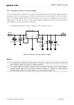
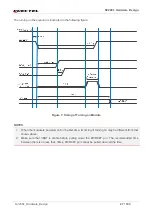
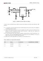
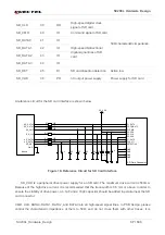
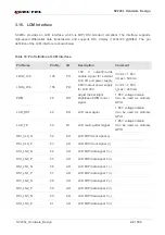
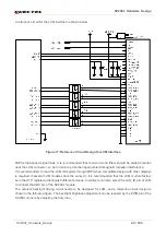
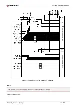
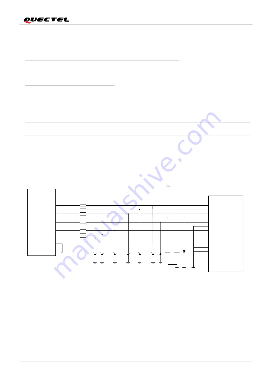
A reference circuit for the SD card interface is shown below.
SD_CMD
SD_DATA3
SD_DATA2
SD_CLK
SD_DATA0
SD_DET
SD_DATA1
P1-DAT2
P2-CD/DAT3
P3-CMD
P4-VDD
P5-CLK
P8-DAT1
GND
P6-VSS
P7-DAT0
DETECTIVE
GND
GND
GND
1
2
3
4
5
6
7
8
9
10
11
12
13
SD_VDD
33R
33R
33R
33R
33R
33R
1K
33 pF
4.7
μ
F
Module
R7
R8
R9
R10
R11
R12
R13
D1
D2
D3
D4
D5
D6
D7
D8
C1
C2
SD Card Connector
GND
Figure 16: Reference Circuit for SD Card Interface
SD_VDD is a peripheral driver power supply for an SD card. The maximum drive current is 500mA.
Because of the high drive current, it is recommended that the trace width is 0.5 mm or above. In order to
ensure the stability of drive power, a 4.7
μ
F and a 33pF capacitor should be added in parallel near the SD
card connector.
CMD, CLK, DATA0, DATA1, DATA2, and DATA3 are all high-speed signal lines. In PCB design, please
control the characteristic impedance of them to 50
Ω
, and do not cross them with other traces. It is
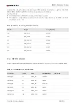
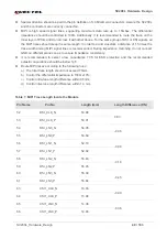
SD_CLK 39 DO
High-speed digital clock
signal of SD card
50
Ω
characteristic impedance
SD_CMD
40
IO
Command signal of SD card
SD_DATA0 41
IO
High-speed bidirectional
digital signal lines of SD
card
SD_DATA1 42
IO
SD_DATA2 43
IO
SD_DATA3 44
IO
SD_DET
45
DI
SD card insertion detection
Active low
SD_VDD
38
PO
3V output power supply
Power supply for SD card


