LPWA Module Series
BG95&BG96 Compatible Design
BG95&BG96_Compatible_Design 14 / 47
1.
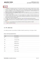
1)
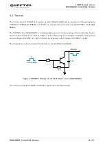
PWRKEY is internally pulled up to an internal voltage in the Qualcomm chipset, and its output
voltage is the internal voltage minus a diode drop in the chipset. For BG95, the expected output
voltage of PWRKEY is 1.5V, and PWRKEY should never be pulled down to GND permanently. For
BG96, the expected output voltage of PWRKEY is 0.8V.
2.
2)
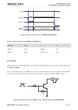
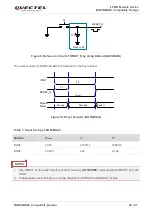
BG95 can be reset by driving RESET_N low for 2s to 3.8s. BG96 can be reset by driving RESET_N
low for 150ms to 460ms.
3.
3)
BG95 supports
ADC0 and ADC1. The two interfaces are internally connected, therefore they
cannot be used simultaneously. If the two ADC interfaces are intended to be used at the same time,
please add an external analog switch.
4.
4)
GNSS_TXD of BG95 is a BOOT_CONFIG pin, and it cannot be pulled up before startup.
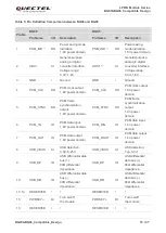
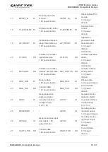
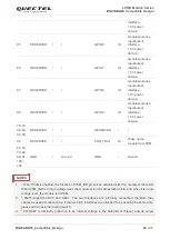
5. The
black
colored pin names are defined for BG95. The
purple
colored pin names are defined for
BG96.
6. The
orange
color indicates the pins with different functions between BG95 and BG96.
7.
“*” means under development.
3.2. Pin Definition
This chapter describes the pin definition of BG95 and BG96 as well as the pin comparison of them.
Table 4: I/O Parameters Definition
Type
Description
AI
Analog input
AO
Analog output
DI
Digital input
DO
Digital output
IO
Bidirectional
OD
Open drain
PI
Power input
PO
Power output
NOTES


