LPWA Module Series
BG95&BG96 Compatible Design
BG95&BG96_Compatible_Design 22 / 47
4
Hardware Reference Designs
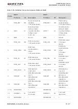
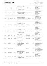
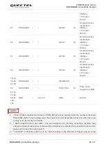
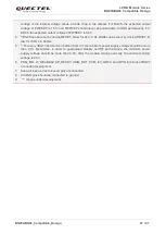
The following chapters describe the compatible design between BG95 and BG96 on main functionalities.
4.1. Power Supply
4.1.1. Reference Design for Power Supply
Power design for a module is critical to its performance. BG95 and BG96 are LPWA modules requiring
low quiescent and leakage current, and also support 2G network. So the power IC must be able to
provide sufficient current output for 2G network.
If the voltage drop between the input and output is not too high, it is recommended to use an LDO to
supply power for the module. If there is a big voltage difference between the input source and the desired
output (VBAT), a buck converter is preferred to be used as the power supply.
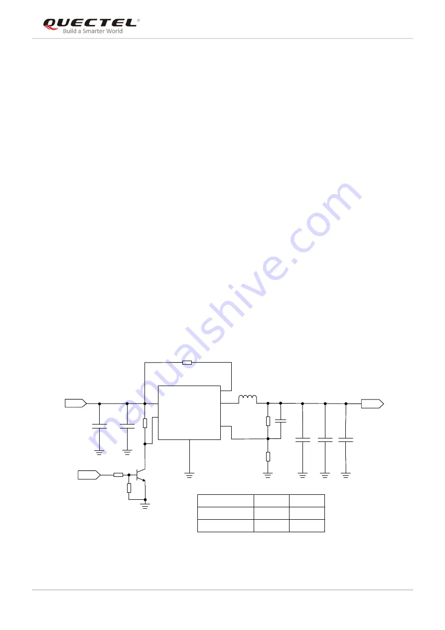
The following is a power supply reference design of BG95/BG96 where buck converter solution is used.
DC_IN
C1
C2
TPS62088
U1
IN
SW
EN
G
N
D
FB
A2
B2
C
2
C1
VBAT
100nF
C4
22
μF
C5
100nF
R2
R3
4.7
μF
51K
R1
MCU_POWER
_ON/OFF
47K
4.7K
R5
R6
Q1
A1
C3
120PF
PG
R4100K 1%
B1
L1
330nH
VBAT=(R2/R3+1)*0.6
BG95-M3/-M4/-M5
BG95-M1/-M2/-N1
R2
R3
536k
Ω 1%
453k
Ω 1%
100k
Ω 1%
100k
Ω 1%
C6
33pF
Figure 2: Reference Circuit of Power Supply (BG95/BG96)

