LTE Module Series
EC20 Mini PCIe Hardware Design
EC20_Mini_PCIe_Hardware_Design Confidential / Released 23 / 36
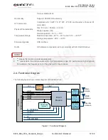
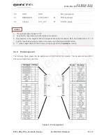
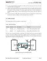
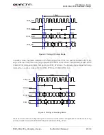
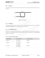
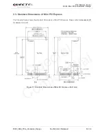
PCM_CLK
PCM_SYNC
PCM_DOUT
MSB
LSB
MSB
MSB
LSB
MSB
PCM_DIN
125us
1
2
256
255
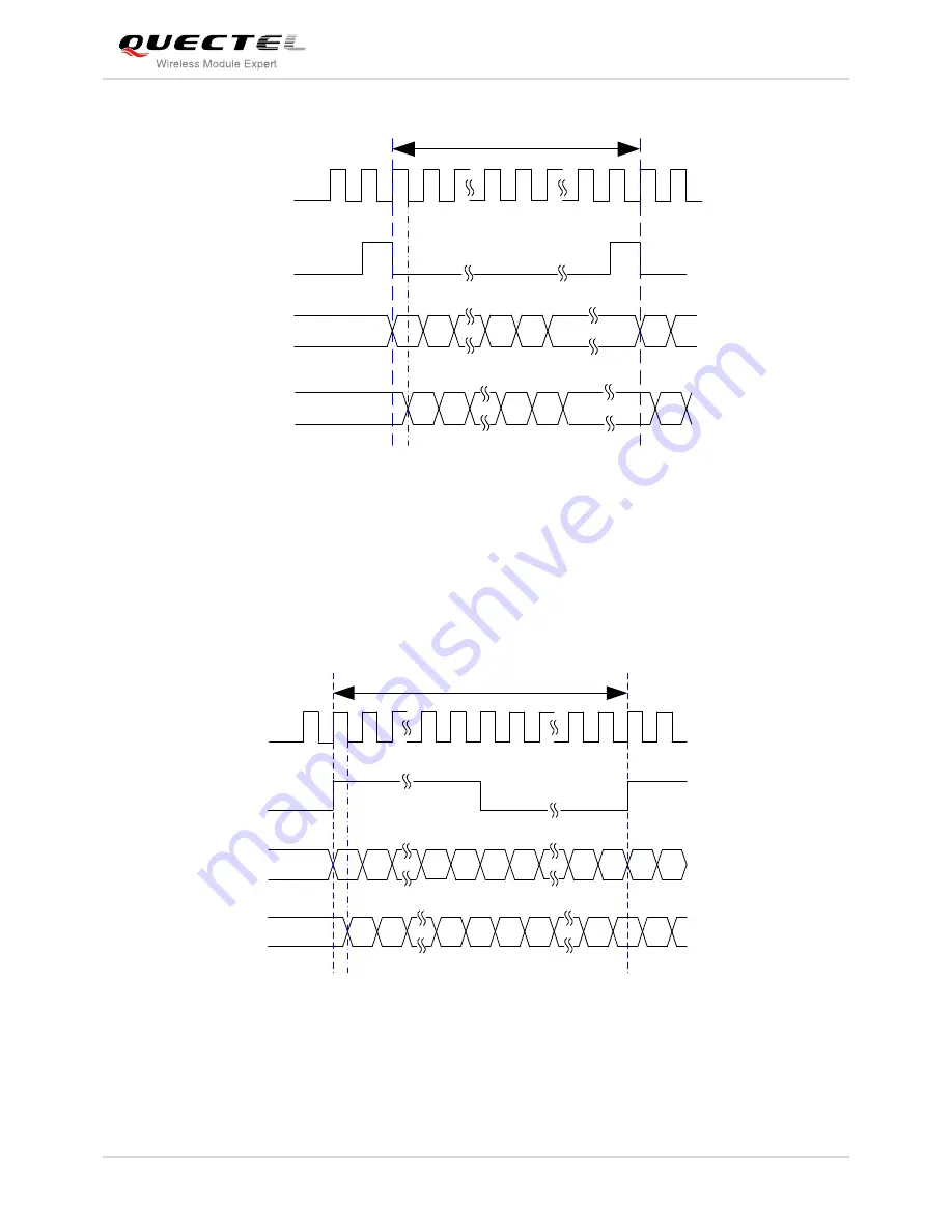
Figure 8: Timing of Primary Mode
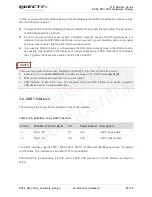
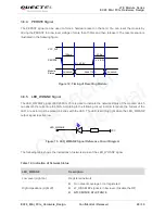
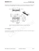
In auxiliary mode, the data is sampled on the falling edge of the PCM_CLK and transmitted on the rising
edge; while the PCM_SYNC rising edge represents the MSB. In this mode, PCM interface operates with a
128kHz PCM_CLK and an 8kHz, 50% duty cycle PCM_SYNC only. The following figure shows the timing
relationship in auxiliary mode with 8kHz PCM_SYNC and 128kHz PCM_CLK.
PCM_CLK
PCM_SYNC
PCM_DOUT
MSB
LSB
PCM_DIN
125us
MSB
1
2
16
15
LSB
Figure 9: Timing of Auxiliary Mode
Clock and mode can be configured by AT command, and the default configuration is master mode using
short sync data format with 2048kHz PCM_CLK and 8kHz PCM_SYNC.
Quectel
Confidential