LTE Standard Module Series
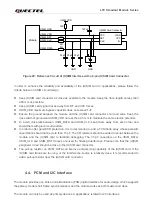
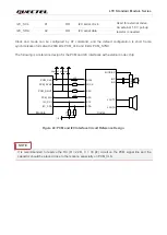
In SD card interface design, in order to ensure good communication performance with SD card, the
following design principles should be complied with:
⚫
The voltage range of SD card power supply VDD_3V is 2.7
–
3.6 V and a sufficient current up to 0.8 A
should be provided. The maximum output current of SD_SDIO_VDD is 50 mA which can only be
used for SDIO pull-up resistors, an externally power supply is needed for SD card.
⚫
To avoid jitter of bus, resistors R7
–
R11 are needed to pull up the SDIO to SD_SDIO_VDD. Value of
these resistors is among 10 k
Ω
to 100 k
Ω and the recommended value is 100
k
Ω. SD_SDIO_VDD
should be used as the pull-up power.
⚫
In order to improve signal quality, it is recommended to add 0 Ω resistors R1 to R6 in series between
the module and the SD card. The bypass capacitors C1 to C6 are reserved and not mounted by
default. All resistors and bypass capacitors should be placed close to the module.
⚫
In order to offer good ESD protection, it is recommended to add a TVS diode on SD card pins near
the SD card connector with junction capacitance less than 15 pF.
⚫
It is important to route the SDIO signal traces with ground surrounded. The impedance of SDIO data
trace is 50
Ω (±10
%).
⚫
Keep SDIO signals far away from other sensitive circuits/signals such as RF circuits, analog signals,
etc., as well as noisy signals such as clock signals, DC-DC signals, etc.
⚫
It is recommended to keep the traces of SD_SDIO_CLK, SD_SDIO_DATA [0:3] and SD_SDIO_CMD
with equal length (the difference among them is less than 1 mm) and the total routing length needs to
be less than 50 mm.
⚫
Make sure the adjacent trace spacing is two times of the trace width and the load capacitance of
SDIO Bus should be less than 15 pF.
4.7. ADC Interface
The module provides two Analog-to-Digital Converter (ADC) interfaces. In order to improve the accuracy
of ADC, the trace of ADC interfaces should be surrounded by ground.
Table 20: Pin Definition of ADC Interface
The voltage value on ADC pins can be read via
AT+QADC=<port>
command:
⚫
AT+QADC=0:
read the voltage value on ADC0
⚫
AT+QADC=1:
read the voltage value on ADC1
Pin Name
Pin No.
I/O
Description
Comment
ADC0
45
AI
General-purpose ADC
interface
If unused, keep it open.
ADC1
44
AI


