background image

PROJECT

TITLE

Lorry XU

Woody WU

CHECKED BY

DRAWN BY

OF

A

6

5

4

3

2

1

SHEET

A

B

C

D

1

2

3

4

5

6

D

C

B

Quectel Wireless Solutions

SIZE

VER

14

9

1.0

DATE

2019/12/5

EG21-G

A2

Reference Design

Handset Application

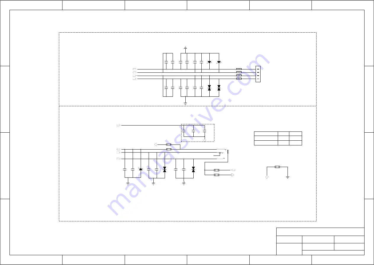
Earphone Application

Close to earphone interface

Notes:

Audio Interfaces

CTIA OMTP

R0702/R0705

R0701/R0704

M

M

NM

NM

1. The analog output only drives earphone and headset. For larger power loads such as speakers, an audio power amplifier should be added in the design.
2. In handset application, both the MIC and SPK signal traces need to be routed as differential pairs.
3. In earphone application, the MIC signal traces need to be routed as differential pairs.
4. All MIC and SPK signal traces should be routed with total grounding and far away from noise such as clock and DC-DC signals, etc. 
5. ALC5616 and TLV320AIC3104 cannot be used simultaneously in audio codec design.

4
1
3
2

J0701

D

0701

ESD9X5.0ST5G

D

0702

C

0702

33pF

C

0704

33pF

C

0705

10pF

C

0703

10pF

C

0706

33pF

C

0701

10pF

C

0709

10pF

C

0710

33pF

C

0711

10pF

C

0712

33pF

C

0708

33pF

C

0707

10pF

C0713

10pF

C0714

33pF

C0715

4.7μF

D

0703

PESD5V0S1BL

D

0704

R0703

0R

R-0805

1

2

3

4
5

J0702

C

0716

10pF

C

0717

33pF

D

0705

ESD

9X5.0ST5G

R0702

NM_0R

R0701

0R

R0704

0R

R0705

NM_0R

D

0706

PESD5V0S1BL

C

0718

10pF

C

0719

33pF

D

0707

PESD5V0S1BL

C

0720

10pF

C

0721

33pF

F0701

0R

F0702

0R

F0704

0R

F0703

0R

[7,8]

SPK_P

[7,8,9] MIC_P
[7,8,9] MIC_N

[7,8,9] MIC_N

[7,8]

SPK_N

[7,8]

SPK_R

[7,8]

SPK_L

[7,8,9] MIC_P

[7,8,9]

MIC_P

Summary of Contents for EG21-G

Page 1: ...EG21 G Reference Design LTE Standard Module Series Rev EG21 G_Reference_Design_V1 0 Date 2019 12 05 Status Released www quectel com...

Page 2: ...RS THE INFORMATION PROVIDED IS BASED UPON CUSTOMERS REQUIREMENTS QUECTEL MAKES EVERY EFFORT TO ENSURE THE QUALITY OF THE INFORMATION IT MAKES AVAILABLE QUECTEL DOES NOT MAKE ANY WARRANTY AS TO THE INF...

Page 3: ...LTE Standard Module Series EG21 G Reference Design EG21 G_Reference_Design 2 8 About the Document Revision History Revision Date Author Description 1 0 2019 12 05 Lim PENG Woody WU Initial...

Page 4: ..._Reference_Design 3 8 Contents About the Document 2 Contents 3 Figure Index 4 1 Reference Design 5 1 1 Introduction 5 1 2 Power on off and Resetting Scenarios 6 1 2 1 Power on Scenario 6 1 2 2 Power o...

Page 5: ...Standard Module Series EG21 G Reference Design EG21 G_Reference_Design 4 8 Figure Index FIGURE 1 TIMING OF TURNING ON MODULE 6 FIGURE 2 TIMING OF TURNING OFF MODULE 7 FIGURE 3 TIMING OF RESETTING MODU...

Page 6: ...8 1 Reference Design 1 1 Introduction This document provides the reference design for Quectel EG21 G module And the reference design includes power on off resetting scenarios block diagrams of power s...

Page 7: ...this time the BOOT_CONFIG pins can be set to high level by external circuit Figure 1 Timing of Turning on Module 1 Please make sure that VBAT is stable before pulling down PWRKEY pin The time between...

Page 8: ...g off Module 1 In order to avoid damaging internal flash please do not switch off the power supply when the module works normally Only after the module is shut down by PWRKEY or AT command the power s...

Page 9: ...e ensure that there is no large capacitance with the max value exceeding 10nF on PWRKEY and RESET_N pins 2 RESET_N only resets the internal baseband chip of the module and does not reset the power man...

Page 10: ...CHECKED BY Woody WU Lorry XU Power Supply Block Diagram DC DC DC 5V OUT e g DC 12V IN DC 3 8V 2 0A EG21 G MIC29302WU MOS ON OFF USB_VBUS EN VBAT_EN SGM2019 ADJYN5G TR DC 3 3V SGM2019 ADJYN5G TR DC 1...

Page 11: ...T_MAIN ADC0 ADC1 MAIN UART I2C ANT_MAIN WAKEUP_IN STATUS NET_MODE NET_STATUS MCU PWRKEY GPIO_03 GPIO_04 RESET_N GPIO_08 GPIO_05 W_DISABLE GPIO_06 USB USB 3 3V 1 8V ALC5616 TLV320AIC3104 or U SIM Card...

Page 12: ...SDC2_CMD 34 VDD_SDIO 35 ANT_DIV 36 GND 37 RESERVED 38 RESERVED 39 RESERVED 40 RESERVED 41 I2C_SCL 42 I2C_SDA 43 RESERVED 44 ADC1 45 ADC0 46 GND 47 ANT_GNSS 48 GND 49 ANT_MAIN 50 GND 51 GND 52 GND 53 G...

Page 13: ...etect the MCU s sleep state For more details please refer to It is used to wake up the module It is used to let the module enter airplane mode 4 WAKEUP_IN_EG21 G should be kept at low level before the...

Page 14: ...o ensure the audio codec Power on Sequence power on VDD_1V8 first then VDD_3 3V Note 1 If VDD_3 3V power supply needs to be switched off please keep CODEC_POWER_EN at high level SGMII It is used when...

Page 15: ...ic capacitance should not be more than 15pF and should be placed close to the U SIM card connector 6 For more information about the layout please refer to For more information about TXS0108E please re...

Page 16: ...D 7 AGND 10 LOUTR N 11 CPN2 12 CPP2 13 CPN1 14 CPP1 15 CPVDD 16 CPVPP 18 CPVREF 19 CPVEE 20 HPO_L 21 ADCDAT1 22 DACDAT1 23 LRCK1 26 SCL 27 SDA 28 GPIO1 IRQ1 29 DBVDD 30 DCVDD 31 MICVDD 32 MICBIAS1 8 V...

Page 17: ...when the surround stereo headphone driver with 32 load is used and is 30mW when the surround stereo headphone driver with 16 load is used 1 MCLK 2 BCLK 3 WCLK 4 DIN 5 DOUT 6 DVSS 7 IOVDD 8 SCL 9 SDA...

Page 18: ...aces need to be routed as differential pairs 4 All MIC and SPK signal traces should be routed with total grounding and far away from noise such as clock and DC DC signals etc 5 ALC5616 and TLV320AIC31...

Page 19: ...to use AT command to turn off diversity reception For more details of the AT command please refer to 3 If an active antenna is selected for the GNSS antenna a VDD power supply circuit is required if...

Page 20: ...close as possible beside the module with a 1 5k pull up resistor away from other signal traces L0901 C0913 and C0914 need to be placed close to Pin 3 2 SGMII data and control signals should be strictl...

Page 21: ...0 and the reference ground of the area should be complete 2 Keep skew of the MDI differential signals less than 20mil and the maximum trace length must be less than10 inches 3 The connection method be...

Page 22: ...sufficient current up to 0 8A needs to be provided 1 The pin 34 VDD_SDIO on the module can only be used for SDIO pull up resistors and its maximum output current is 50mA Notes The bypass capacitors C...

Page 23: ...is in sleep replace the power supply of indicators with controllable one 4 The module s debug UART interface supports 1 8V power domain Turn off the power when the module enters sleep mode 1 It is rec...

Reviews: