
Wi-Fi&BT Module Series
FC21 Hardware Design
FC21_Hardware_Design 16 / 52
pin open.
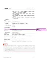
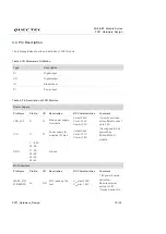
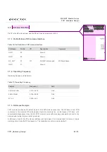
WLAN_EN
9
DI
Wi-Fi function
control
V
IL
min=-0.3V
V
IL
max=0.54V
V
IH
min=1.26V
V
IH
max=2.0V
1.8V power domain.
Active high.
SDIO_D3
22
IO
SDIO data bus D3
V
OL
max=0.18V
V
OH
min=1.62V
V
IL
min=-0.3V
V
IL
max=0.54V
V
IH
min=1.26V
V
IH
max=2.0V
1.8V power domain
SDIO_D2
1)
23
IO
SDIO data bus D2
V
OL
max=0.18V
V
OH
min=1.62V
V
IL
min=-0.3V
V
IL
max=0.54V
V
IH
min=1.26V
V
IH
max=2.0V
1.8V power domain.
Require external
pull-up to 1.8V.
SDIO_D1
24
IO
SDIO data bus D1
V
OL
max=0.18V
V
OH
min=1.62V
V
IL
min=-0.3V
V
IL
max=0.54V
V
IH
min=1.26V
V
IH
max=2.0V
1.8V power domain
SDIO_D0
25
IO
SDIO data bus D0
V
OL
max=0.18V
V
OH
min=1.62V
V
IL
min=-0.3V
V
IL
max=0.54V
V
IH
min=1.26V
V
IH
max=2.0V
1.8V power domain
SDIO_CLK
26
DI
SDIO bus clock
V
IL
min=-0.3V
V
IL
max=0.54V
V
IH
min=1.26V
V
IH
max=2.0V
1.8V power domain
SDIO_CMD
27
IO
SDIO bus command
V
OL
max=0.18V
V
OH
min=1.62V
V
IL
min=-0.3V
V
IL
max=0.54V
V
IH
min=1.26V
V
IH
max=2.0V
1.8V power domain
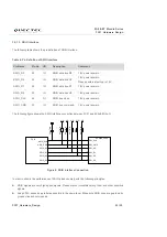
BT Interface
Pin Name
Pin No.
I/O
Description
DC Characteristics
Comment


