Wi-Fi&BT Module Series
FC21 Hardware Design
FC21_Hardware_Design 22 / 52
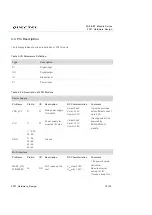
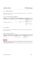
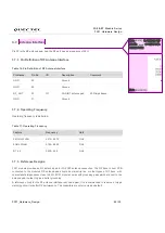
3.5.1.3. SDIO Interface
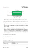
The following table shows the pin definition of SDIO interface.
Table 8: Pin Definition of SDIO Interface
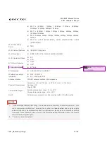
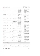
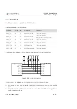
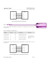
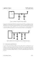
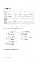
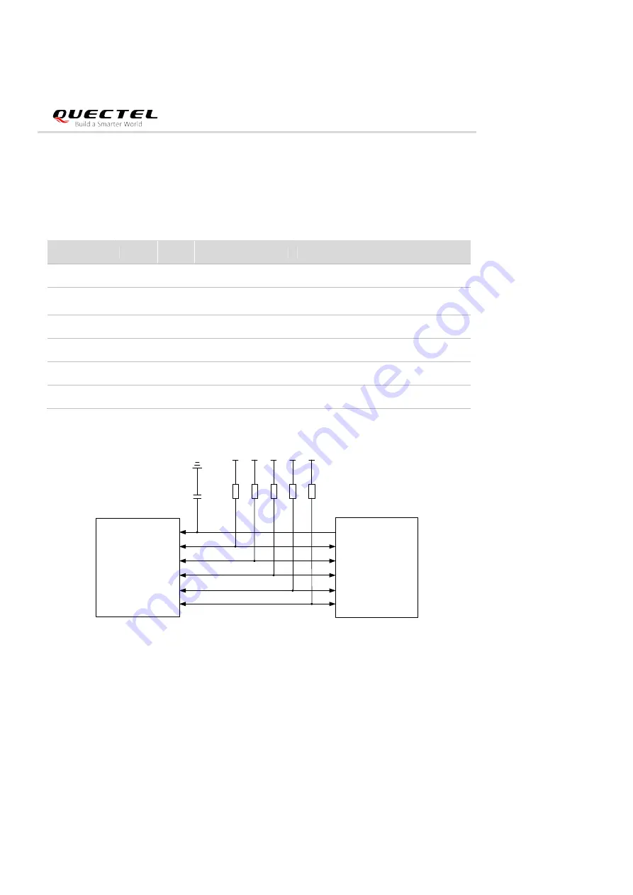
The following figure shows the SDIO interface connection between FC21 and EC2x&EG2x-G.
SDIO_CLK
SDIO_CMD
SDIO_D0
SDIO_D1
SDIO_D2
SDIO_D3
EC2x&EG2x-G
FC21
SD1_D0
SD1_D1
SD1_D2
SD1_D3
SD1_CLK
SD1_CMD
1
0
K
VIO
VIO
VIO
VIO
VIO
N
M
_
1
0
K
N
M
_
1
0
K
N
M
_
1
0
K
N
M
_
1
0
K
N
M
_
1
0
p
F
Figure 6: SDIO Interface Connection
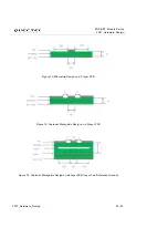
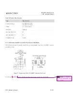
In order to ensure the performance of SDIO, please comply with the following principles:
SDIO signals are very high-speed signals. Please prevent crosstalk among them and other sensitive
signals.
Keep SDIO traces as parallel as possible in the same layer. Make sure SDIO lines are guarded by
ground vias and not crossed.
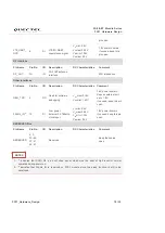
Pin Name
Pin No. I/O
Description
Comment
SDIO_D3
22
IO
SDIO data bus D3
1.8V power domain.
SDIO_D2
23
IO
SDIO data bus D2
1.8V power domain.
Require external pull-up to 1.8V.
SDIO_D1
24
IO
SDIO data bus D1
1.8V power domain.
SDIO_D0
25
IO
SDIO data bus D0
1.8V power domain.
SDIO_CLK
26
DI
SDIO bus clock
1.8V power domain.
SDIO_CMD
27
IO
SDIO
bus command
1.8V power domain.