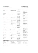
Wi-Fi&BT Module Series
FC21 Hardware Design
FC21_Hardware_Design 23 / 52
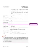
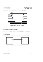
Do not route SDIO signal traces under crystals, oscillators, magnetic devices and RF signal traces.
SDIO_D2 is a boot strap signal, which must be kept at high level for normal operation during power
on. The pull-up resistor on SDIO_D2 line must be mounted.
Keep SDIO traces as short as possible with equal length, and impedance control as 50Ω.
The spacing to all other signals is greater than 2 times of the trace width.
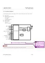
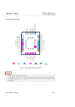
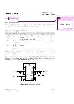
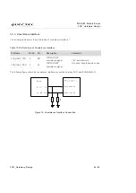
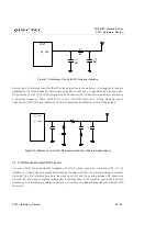
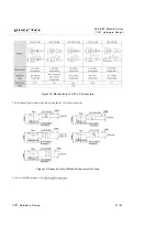
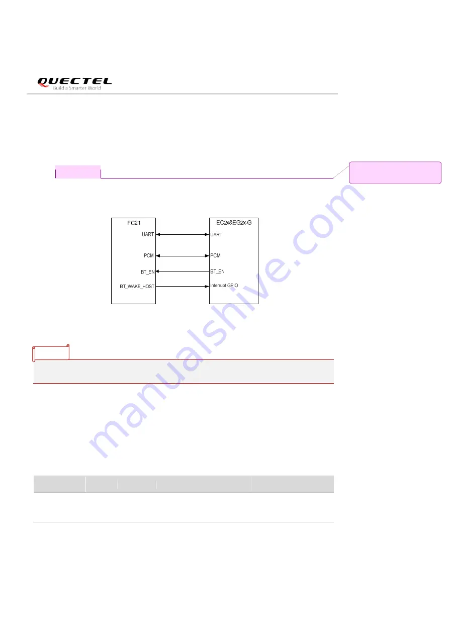
3.5.2. BT Interface*
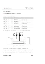
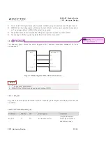
The following figure shows the block diagram of BT interface connection between FC21 and
EC2x&EG2x-G.
Figure 7: Block Diagram of BT Interface Connection
1. “*” means under development.
2. PIN3 of EC2x / EG2x-G can be used as an interrupt GPIO.
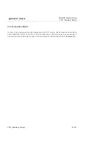
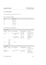
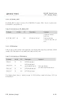
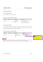
3.5.2.1. BT_EN
BT_EN is used to control the BT function of FC21. When BT_EN is at high level voltage, BT function will
be enabled.
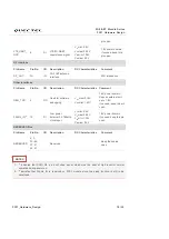
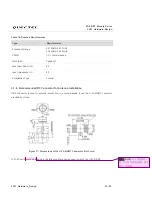
Table 9: Pin Definition of BT_EN
Pin Name
Pin No.
I/O
Description
Comment
BT_EN
10
DI
BT function control
1.8V power domain.
Active high. If unused,
keep this pin open.
NOTES
批注
[RL8]:
中文这里没有加星
号,中文是否要加上