background image


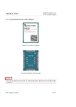
Wi-Fi&BT  Module  Series 

                                                                                                                            FC21  Hardware  Design


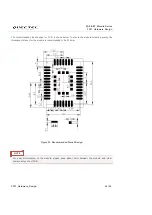
FC21_Hardware_Design                                                                                                                              48 / 52 


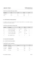
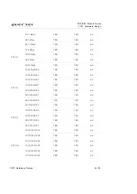
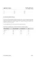
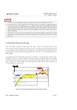
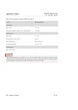
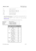
Table 31: Recommended Thermal Profile Parameters 


During  manufacturing  and  soldering,  or  any  other  processes  that  may  contact  the  module  directly, 

NEVER wipe the module label with organic solvents, such as acetone, ethyl alcohol, isopropyl alcohol, 

trichloroethylene, etc. Otherwise, the label information may become unclear.   


Factor 

Recommendation 

Soak Zone 


Max slope 

1–3 °C/s 

Soak time (between A and B: 150 °C and 200 °C) 

70–120 s 

Reflow Zone 


Max slope 

2–3 °C/s 

Reflow time (D: over 220°C) 

45–70 s 

Max temperature 

238 °C to 246 °C 

Cooling down slope 

-1.5 to -3 °C/s 

Reflow Cycle 


Max reflow cycle   

NOTE 

Summary of Contents for FC21

Page 1: ...FC21 Hardware Design Wi Fi BT Module Series Version 1 0 Date 2020 08 13 Status Preliminary www quectel com ...

Page 2: ...SE OF OR RELIANCE UPON THE INFORMATION ALL INFORMATION SUPPLIED HEREIN IS SUBJECT TO CHANGE WITHOUT PRIOR NOTICE DISCLAIMER WHILE QUECTEL HAS MADE EFFORTS TO ENSURE THAT THE FUNCTIONS AND FEATURES UNDER DEVELOPMENT ARE FREE FROM ERRORS IT IS POSSIBLE THAT THESE FUNCTIONS AND FEATURES COULD CONTAIN ERRORS INACCURACIES AND OMISSIONS UNLESS OTHERWISE PROVIDED BY VALID AGREEMENT QUECTEL MAKES NO WARRA...

Page 3: ...Wi Fi BT Module Series FC21 Hardware Design FC21_Hardware_Design 2 52 About the Document Revision History Version Date Author Description 1 0 2020 08 13 Power JIN Kris ZHANG Initial ...

Page 4: ...oduction 19 3 5 Wireless Connectivity Interfaces 20 3 5 1 Wi Fi Interface 20 3 5 1 1 WAKE_ON_WIRELESS 21 3 5 1 2 WAKE_EN 21 3 5 1 3 SDIO Interface 22 3 5 2 BT Interface 23 3 5 2 1 BT_EN 23 3 5 2 2 BT_WAKE_HOST 24 3 5 2 3 PCM Interface 24 3 5 2 4 BT_UART Interface 25 3 5 3 Coexistence Interface 26 3 6 Other Interfaces 27 3 6 1 DBG_TXD Interface 27 3 6 2 32KHz_IN Interface 27 3 7 Antenna Interface 2...

Page 5: ... Fi Current Consumption 35 4 4 2 BLE Current Consumption 37 4 5 RF Performance 37 4 5 1 Wi Fi Performance 37 4 5 2 BLE Performance 39 4 6 Electrostatic Discharge 40 5 Mechanical Dimensions 41 5 1 Mechanical Dimensions of the Module 41 5 2 Recommended Footprint and Stencil Design 43 5 3 Top and Bottom Views of the Module 45 6 Storage Manufacturing and Packaging 46 6 1 Storage 46 6 2 Manufacturing a...

Page 6: ...on of 32KHz_IN Interface 27 Table 16 Pin Definition of RF Antenna Interface 28 Table 17 Operating Frequency 28 Table 18 Antenna Cable Requirements 31 Table 19 Antenna Requirements 32 Table 20 Absolute Maximum Ratings 34 Table 21 Recommended Operating Conditions 35 Table 22 General DC Electrical Characteristics 35 Table 23 Wi Fi Current Consumption 35 Table 24 BLE Current Consumption During Non sig...

Page 7: ...Circuit for RF Antenna Interface Vehicle Applications 29 Figure 13 Microstrip Design on a 2 layer PCB 30 Figure 14 Coplanar Waveguide Design on a 2 layer PCB 30 Figure 15 Coplanar Waveguide Design on a 4 layer PCB Layer 3 as Reference Ground 30 Figure 16 Coplanar Waveguide Design on a 4 layer PCB Layer 4 as Reference Ground 31 Figure 17 Dimensions of the U FL R SMT Connector Unit mm 32 Figure 18 M...

Page 8: ...ickly understand module interface specifications electrical and mechanical details as well as other related information of the module In combination with Quectel EC2x EG2X G1 modules FC21 module can help customers to design and set up LTE Wi Fi BT applications easily Table 1 FC21 Module 1 In this document EC2x refers to Quectel EC25 EC21 and EC20 R2 1 modules and EG2x G refers to Quectel EG21 G an...

Page 9: ... may cause interference on sensitive medical equipment so please be aware of the restrictions on the use of wireless devices when in hospitals clinics or other healthcare facilities Cellular terminals or mobiles operating over radio signal and cellular network cannot be guaranteed to connect in certain conditions such as when the mobile bill is unpaid or the U SIM card is invalid When emergent hel...

Page 10: ...kage is compact and the size is only 16 6mm 13mm 2 1mm 1 means under development 2 BLE function of FC21 module is available 2 2 Key Features The following table describes the detailed features of FC21 module Table 2 Key Features Features Description Power Supply VDD_3V3 Power Supply Voltage Range 3 14V 3 46V Typical voltage 3 3V I O supply voltage Voltage Range 1 71V 3 46V Typical voltage 1 8V Wi ...

Page 11: ...0Mbps 45Mbps 60Mbps 90Mbps 120Mbps 150Mbps 802 11a 6Mbps 9Mbps 12Mbps 18Mbps 24Mbps 36Mbps 48Mbps 54Mbps 802 11ac VHT20 MCS0 MCS8 VHT40 MCS0 MCS9 VHT80 MCS0 MCS9 Wi Fi Transmitting Power TBD Wi Fi Protocol Features IEEE 802 11a b g n ac Wi Fi Modulation BPSK QPSK CCK 16QAM 64QAM 256QAM Wi Fi Operation Modes AP STA BT Protocol Features GATT SPP BT Operation Modes BT BLE BT Modulation GFSK 8 DPSK π ...

Page 12: ...ajor functional parts Power supply Wireless Connectivity Interfaces Wi Fi interface BT interface Coexistence interface Antenna interface Other interfaces DBG_TXD 32KHz_IN interface Figure 1 Functional Diagram of FC21 Module FC21_SA version has 2 4G Filter FC21_SD version does not have 2 4G Filter NOTE 批注 RL5 FC21_SA 版本带 2 4G Filter FC21_SD版本不带2 4G Filter 要不要加这个备注 批注 RL6R5 ...

Page 13: ...ard In order to help customers to develop applications with FC21 module Quectel supplies an evaluation board UMTS LTE EVB an RS 232 to USB converter cable a USB data cable a power adapter 4 antennas and other peripherals to control or test the module For details please refer to document 1 ...

Page 14: ... with 38 LCC pads and 14 LGA pads that can be connected to cellular application platform The subsequent chapters will provide detailed descriptions of the following interfaces Power supply Wireless Connectivity Interfaces Wi Fi interface BT interface Coexistence interface Other interfaces DBG_TXD interface 32KHz_IN interface Antenna interface ...

Page 15: ...E_UART_RXD BT_UART_RTS 1 3 4 2 1 5 6 8 9 7 10 11 12 51 50 52 40 39 41 42 44 45 43 PCM_IN 1 PCM_SYNC 1 PCM_CLK 1 PCM_OUT 1 BT_UART_TXD 1 BT_UART_RXD 1 32KHz_IN 2 GND GND RESERVED RESERVED RESERVED RESERVED WAKE_ON_WIRELESS Power GND WLAN Reserved Other signals RF BT Figure 2 Pin Assignment of FC21 Module 1 Please keep all RESERVED pins open 2 1 indicates that pins 7 8 10 13 18 and 46 are BT functio...

Page 16: ...racteristics Comment VDD_3V3 21 PI Main power supply for module Vmax 3 46V Vmin 3 14V Vnorm 3 3V It must be provided with sufficient current up to 0 6A VIO 11 PI Power supply for module s I O pins Vmax 3 46V Vmin 1 71V Vnorm 1 8V It is suggested to be powered by EC2x EG2x G module GND 1 12 20 28 29 31 36 38 40 43 45 48 52 Ground Wi Fi Interface Pin Name Pin No I O Description DC Characteristics Co...

Page 17: ...1 26V VIHmax 2 0V 1 8V power domain Require external pull up to 1 8V SDIO_D1 24 IO SDIO data bus D1 VOLmax 0 18V VOHmin 1 62V VILmin 0 3V VILmax 0 54V VIHmin 1 26V VIHmax 2 0V 1 8V power domain SDIO_D0 25 IO SDIO data bus D0 VOLmax 0 18V VOHmin 1 62V VILmin 0 3V VILmax 0 54V VIHmin 1 26V VIHmax 2 0V 1 8V power domain SDIO_CLK 26 DI SDIO bus clock VILmin 0 3V VILmax 0 54V VIHmin 1 26V VIHmax 2 0V 1...

Page 18: ...ILmax 0 54V VIHmin 1 26V VIHmax 2 0V 1 8V power domain If unused keep this pin open PCM_OUT 16 DO BT PCM data output VOLmax 0 18V VOHmin 1 62V 1 8V power domain If unused keep this pin open BT_UART_ RTS 7 DO BT UART request to send VOLmax 0 18V VOHmin 1 62V 1 8V power domain If unused keep this pin open BT_UART_ CTS 8 DI BT UART clear to send VILmin 0 3V VILmax 0 54V VIHmin 1 26V VIHmax 2 0V 1 8V ...

Page 19: ... open RF Interface Pin Name Pin No I O Description DC Characteristics Comment RF_ANT 30 IO Wi Fi BT antenna interface 50Ω impedance Other Interfaces Pin Name Pin No I O Description DC Characteristics Comment DBG_TXD 4 OD Used for software debugging VOLmax 0 18V VOHmin 1 62V 1 8V power domain Require external pull up to 1 8V If unused keep this pin open 32KHz_IN 2 19 DI Low power External 32 768kHz...

Page 20: ...o a high voltage level will enable VDD_3V3 power output And this pin should be connected to pin 127 of EC2x EG2x G For more details please refer to document 2 3 4 5 or 6 TPS630242 L1 L1 L2 L2 VIN VIN VIN VINA GND EN VOUT VOUT VOUT PFM PWM FB PGND D2 D3 E1 E2 E3 E4 C4 D1 B1 A1 L1 L2 PGND PGND U402 D4 B2 B3 A2 A3 A4 B4 C1 C2 C3 C406 R408 C405 10 µF 1M L401 1 µH R407 100K 22 µF C407 22 µF PM_ENABLE D...

Page 21: ..._ENABLE 0 0 VIO 0 10 µs Figure 4 Timing of Turning on off FC21 Module 3 5 Wireless Connectivity Interfaces FC21 support a low power SDIO 3 0 interface for WLAN and UART PCM interfaces for BT function 3 5 1 Wi Fi Interface The following figure shows the WLAN interface connection between FC21 and EC2x EG2x G EC2x EG2x G FC21 SDIO WLAN_EN WLAN_EN WAKE_ON_WIRELESS WAKE_ON_WIRELESS SDIO Figure 5 Wi Fi ...

Page 22: ...FC21 When WLAN_EN is at high level voltage Wi Fi function will be enabled Table 7 Pin Definition of WLAN_EN WLAN_EN is a sensitive signal and therefore WLAN_EN should be ground shielded and routed as close as possible to FC21 module Pin Name Pin No I O Description Comment WAKE_ON_WIRELESS 32 OD Wi Fi wake up the host 1 8V power domain Active low Require external pull up to 1 8V If unused keep this...

Page 23: ...tion In order to ensure the performance of SDIO please comply with the following principles SDIO signals are very high speed signals Please prevent crosstalk among them and other sensitive signals Keep SDIO traces as parallel as possible in the same layer Make sure SDIO lines are guarded by ground vias and not crossed Pin Name Pin No I O Description Comment SDIO_D3 22 IO SDIO data bus D3 1 8V powe...

Page 24: ...ther signals is greater than 2 times of the trace width 3 5 2 BT Interface The following figure shows the block diagram of BT interface connection between FC21 and EC2x EG2x G Figure 7 Block Diagram of BT Interface Connection 1 means under development 2 PIN3 of EC2x EG2x G can be used as an interrupt GPIO 3 5 2 1 BT_EN BT_EN is used to control the BT function of FC21 When BT_EN is at high level vo...

Page 25: ... pin open 3 5 2 3 PCM Interface FC21 provides a PCM interface for BT application The following table shows the pin definition of PCM interface The PCM interface is not needed when a BLE function is used Table 11 Pin Definition of PCM Interface Pin Name Pin No I O Description Comment PCM_IN 13 DI BT PCM data input 1 8V power domain If unused keep these pins open PCM_SYNC 14 DI BT PCM data frame syn...

Page 26: ...Definition of UART Interface The following figure shows a reference design for UART interface connection between FC21 and EC2x EG2x G Figure 9 Reference Design for UART Interface Connection Pin Name Pin No I O Description Comment BT_UART_RTS 7 DO BT UART request to send 1 8V power domain If unused keep these pins open BT_UART_CTS 8 DI BT UART clear to send BT_UART_TXD 17 DO BT UART transmit data B...

Page 27: ...Table 13 Pin Definition of Coexistence Interface The following figure shows the coexistence interface connection between FC21 and EC2x EG2x G Figure 10 Coexistence Interface Connection Pin Name Pin No I O Description Comment LTE_UART_TXD 5 DO LTE Wi Fi BT coexistence signal 1 8V power domain If unused keep these pins open LTE_UART_RXD 6 DI LTE Wi Fi BT coexistence signal ...

Page 28: ...cons in various power saving schemes and to maintain basic logic operations in sleep mode Table 15 Pin Definition of 32KHz_IN Interface 32KHz_IN pin is reserved on FC21 module since the sleep function is still to be developed Pin Name Pin No I O Description Comment DBG_TXD 4 OD Used for software debugging 1 8V power domain Require external pull up to 1 8V If unused keep this pin open Pin Name Pin ...

Page 29: ...s RF antenna pad should be microstrip line or other types of RF trace with characteristic impendence close to 50Ω FC21 module comes with grounding pads which are next to the antenna pad in order to give a better grounding A reference circuit for the RF antenna interface is shown below It is recommended to reserve a π type matching circuit for better RF performance The capacitors are not mounted by...

Page 30: ...e a π type matching circuit Capacitors C1 C2 C3 C4 and inductors L1 L3 are not mounted by default and L2 is 0Ω by default Figure 12 Reference Circuit for RF Antenna Interface Vehicle Applications 3 7 4 Reference Design of RF Layout For user s PCB the characteristic impedance of all RF traces should be controlled to 50 Ω The impedance of the RF traces is usually determined by the trace width W the ...

Page 31: ...C21 Hardware Design FC21_Hardware_Design 30 52 Figure 13 Microstrip Design on a 2 layer PCB Figure 14 Coplanar Waveguide Design on a 2 layer PCB Figure 15 Coplanar Waveguide Design on a 4 layer PCB Layer 3 as Reference Ground ...

Page 32: ...changed to curved ones The recommended trace angle is 135 There should be clearance under the signal pin of the antenna connector or solder joint The reference ground of RF traces should be complete Meanwhile adding some ground vias around RF traces and the reference ground could help to improve RF performance The distance between the ground vias and RF traces should be no less than two times the ...

Page 33: ...ed to use the U FL R SMT connector provided by Hirose Figure 17 Dimensions of the U FL R SMT Connector Unit mm U FL LP serial connectors listed in the following figure can be used to match the U FL R SMT Type Requirements Frequency Range 2 412GHz 2 472GHz 5 180GHz 5 825GHz VSWR 2 1 recommended Gain dBi Typically 1 Max Input Power W 50 Input Impedance Ω 50 Polarization Type Vertical 批注 RL14 这个是连接器 ...

Page 34: ...ign FC21_Hardware_Design 33 52 Figure 18 Mechanicals of U FL LP Connectors The following figure describes the space factor of mated connector Figure 19 Space Factor of Mated Connector Unit mm For more details please visit http www hirose com ...

Page 35: ...e listed in detail in the following chapters Electrical characteristics I O interface characteristics Current consumption RF performance Electrostatic discharge 4 2 Electrical Characteristics The following table shows the absolute maximum ratings Table 20 Absolute Maximum Ratings The following table shows the recommended operating conditions for FC21 module Parameter Min Max Unit VDD_3V3 0 3 3 46 ...

Page 36: ...rent Consumption 4 4 1 Wi Fi Current Consumption Table 23 Wi Fi Current Consumption Parameter Min Typ Max Unit VDD_3V3 3 14 3 3 3 46 V VIO 1 71 1 8 3 46 V Symbol Parameter Min Max Unit VIH High Level Input Voltage 0 7 x VIO VIO 0 2 V VIL Low Level Input Voltage 0 3 0 3 x VIO V VOH High Level Output Voltage 0 9 x VIO VIO V VOL Low Level Output Voltage 0 0 1 x VIO V IIL Input Leakage Current 5 5 μA ...

Page 37: ... MCS0 TBD TBD mA TX HT20 MCS7 TBD TBD mA TX HT40 MCS0 TBD TBD mA TX HT40 MCS7 TBD TBD mA RX HT20 MCS0 TBD TBD mA RX HT20 MCS7 TBD TBD mA RX HT40 MCS0 TBD TBD mA RX HT40 MCS7 TBD TBD mA 802 11a TX HT20 MCS0 TBD TBD mA TX HT20 MCS7 TBD TBD mA RX HT20 MCS0 TBD TBD mA RX HT20 MCS7 TBD TBD mA TX VHT20 MCS0 TBD TBD mA 802 11ac TX VHT20 MCS8 TBD TBD mA TX VHT40 MCS0 TBD TBD mA TX VHT40 MCS9 TBD TBD mA TX...

Page 38: ...4 BLE Current Consumption During Non signaling 4 5 RF Performance 4 5 1 Wi Fi Performance The following tables summarize the transmitter and receiver characteristics of FC20 series Table 25 Conducted RF Output Power at 2 4GHz RX VHT20 MCS0 TBD TBD mA RX VHT20 MCS8 TBD TBD mA RX VHT40 MCS0 TBD TBD mA RX VHT40 MCS9 TBD TBD mA RX VHT80 MCS8 TBD TBD mA RX VHT80 MCS9 TBD TBD mA Description Power Power ...

Page 39: ...2 11n HT40 MCS0 TBD dBm 802 11n HT40 MCS7 TBD dBm Standard Data Rate Typ Unit 802 11a 6 Mbps TBD dBm 802 11a 54 Mbps TBD dBm 802 11n HT20 MCS0 TBD dBm 802 11n HT20 MCS7 TBD dBm 802 11n HT40 MCS0 TBD dBm 802 11n HT40 MCS7 TBD dBm 802 11ac VHT20 MCS0 TBD dBm 802 11ac VHT20 MCS8 TBD dBm 802 11ac VHT40 MCS0 TBD dBm 802 11ac VHT40 MCS9 TBD dBm 802 11ac VHT80 MCS0 TBD dBm 802 11ac VHT80 MCS9 TBD dBm Sta...

Page 40: ...g 6Mbps TBD dBm 802 11g 54Mbps TBD dBm 802 11n HT20 MCS0 TBD dBm 802 11n HT20 MCS7 TBD dBm 802 11n HT40 MCS0 TBD dBm 802 11n HT40 MCS7 TBD dBm Standard Data Rate Typ Unit 802 11a 6 Mbps TBD dBm 802 11a 54 Mbps TBD dBm 802 11n HT20 MCS0 TBD dBm 802 11n HT20 MCS7 TBD dBm 802 11n HT40 MCS0 TBD dBm 802 11n HT40 MCS7 TBD dBm 802 11ac VHT20 MCS0 TBD dBm 802 11ac VHT20 MCS8 TBD dBm 802 11ac VHT40 MCS0 TB...

Page 41: ...D sensitive components Proper ESD handling and packaging procedures must be followed throughout the processing handling and operation of any application that involves the module The following table shows the module s electrostatic discharge characteristics Table 30 Electrostatic Discharge Characteristics 25ºC 45 Relative Humidity 19 TBD TBD 39 TBD TBD Tested Interfaces Contact Discharge Air Discha...

Page 42: ...chanical Dimensions This chapter describes the mechanical dimensions of FC21 module All dimensions are measured in millimeter mm and the dimensional tolerances are 0 05mm unless otherwise specified 5 1 Mechanical Dimensions of the Module Pin 1 Figure 20 Top and Side Dimensions ...

Page 43: ...Wi Fi BT Module Series FC21 Hardware Design FC21_Hardware_Design 42 52 Figure 21 Bottom Dimensions The package warpage level of the module conforms to JEITA ED 7306 standard NOTE ...

Page 44: ...Wi Fi BT Module Series FC21 Hardware Design FC21_Hardware_Design 43 52 5 2 Recommended Footprint and Stencil Design Figure 22 Recommended Footprint 批注 RL15 中文分开的两章 结 是否需要分开 ...

Page 45: ...cil design for FC21 is shown below To ensure the module soldering quality the thickness of stencil for the module is recommended to be 0 18mm Figure 23 Recommended Stencil Design For easy maintenance of the module please keep about 3mm between the module and other components on host PCB NOTE ...

Page 46: ...C21_Hardware_Design 45 52 5 3 Top and Bottom Views of the Module Figure 24 Top View of the Module Figure 25 Bottom View of the Module These are renderings of FC21 modules For authentic appearance please refer to the module provided by Quectel NOTE ...

Page 47: ...odule must be processed in reflow soldering or other high temperature operations within 168 hours Otherwise the module should be stored in an environment where the relative humidity is less than 10 e g a drying cabinet 4 The module should be pre baked to avoid blistering cracks and inner layer separation in PCB under the following circumstances The module is not stored in Recommended Storage Condi...

Page 48: ...sh the squeegee to apply the solder paste on the surface of stencil thus making the paste fill the stencil openings and then penetrate to the PCB The force on the squeegee should be adjusted properly so as to produce a clean stencil surface on a single pass To ensure the module soldering quality the thickness of stencil for the module is recommended to be 0 15 0 18 mm For more details please refer...

Page 49: ...e the module label with organic solvents such as acetone ethyl alcohol isopropyl alcohol trichloroethylene etc Otherwise the label information may become unclear Factor Recommendation Soak Zone Max slope 1 3 C s Soak time between A and B 150 C and 200 C 70 120 s Reflow Zone Max slope 2 3 C s Reflow time D over 220 C 45 70 s Max temperature 238 C to 246 C Cooling down slope 1 5 to 3 C s Reflow Cycl...

Page 50: ...Hardware_Design 49 52 6 3 Packaging FC21 module is packaged in a vacuum sealed bag which is ESD protected The bag should not be opened until the devices are ready to be soldered onto the application Figure 27 Tape Dimensions Figure 28 Reel Dimensions ...

Page 51: ...eference design 4 Quectel_EC20_R2 1_Reference_Design EC20 R2 1 reference design 5 Quectel_EG25 G_Reference_Design EC25 G reference design 6 Quectel_EG21 G_Reference_Design EC21 G reference design 7 Quectel_RF_Layout_Application_Note RF layout application note 8 Quectel_Module_Secondary_SMT_User_Guide Module secondary SMT user guide Abbreviation Description AP Access Point BPSK Binary Phase Shift K...

Page 52: ...Board QAM Quadrature Amplitude Modulation QPSK Quadrature Phase Shift Keying RF Radio Frequency RH Relative Humidity RoHS Restriction of Hazardous Substances RX Receive Direction SDIO Secure Digital Input and Output Card STA Station TX Transmitting Direction USB Universal Serial Bus VDD Voltage Power for Digital Device VHT Very High Throughput VIHmax Maximum Input High Level Voltage Value VIHmin M...

Page 53: ...9 dbm rate conducted power WIFI 5G 17 dbm rate conducted power External antenna gain Band Antenna Gain dBi Wi Fi 2 4G 802 11b 5 16 802 11g 5 16 802 11n HT20 5 16 802 11n HT40 5 16 Wi Fi 5G U NII 1 802 11a 4 48 802 11n HT20 4 48 802 11n HT40 4 48 802 11ac HT20 4 48 802 11ac HT40 4 48 802 11ac HT80 4 48 Wi Fi 5G U NII 2A 802 11a 4 48 802 11n HT20 4 48 802 11n HT40 4 48 802 11ac HT20 4 48 802 11ac HT...

Page 54: ...lowing statements must be attached to the host end product This device contains FCC ID XMR202102FC21 4 This module must not transmit simultaneously with any other antenna or transmitter 5 The host end product must include a user manual that clearly defines operating requirements and conditions that must be observed to ensure compliance with current FCC RF exposure guidelines For portable devices i...

Page 55: ...ch as on a computer disk or over the Internet the information required by this section may be included in the manual in that alternative form provided the user can reasonably be expected to have the capability to access information in that form This device complies with part 15 of the FCC Rules Operation is subject to the following two conditions 1 This device may not cause harmful interference an...

Reviews: