background image

L50 Hardware Design                                                                                                                   


L50_HD_V1.0                                                                                                                                                                -14-


ON_OFF    4 

Power control 

pin 

VILmin=-0.4V 

VILmax=0.45V 

VIHmin=0.7* 

VIO/RTC 

VIHmax=3.6V 


A  pulse  generated  on  the 

ON_OFF  pin  which  lasts 

for  at  least  1ms  and 

consists  of  a  rising  edge 

and  low  level,  can  switch 

operating  mode  between 

hibernate and full-on. 

1PPS 

One pulse per 

second 

VOLmin=-0.3V 

VOLmax=0.4V 

VOHmin=0.75*VCC 

1PPS  output  provides  a 

pulse  signal  for  time 

purpose.  If  unused,  leave 

this pin unconnected. 

Serial Interface 

PIN 

NAME 

PIN   

NO. 

I/

DESCRIPTIO

DC 

CHARACTERISTICS 

COMMENT 

DR_I2CD

IO 

21 


I/

Dead Reckoning 

I2C data (SDA) 


VOLmax=0.4V 

VOHmin=0.75*VCC 

VILmin=-0.4V 

VILmax=0.45V 

VIHmin=0.7*VCC 

VIHmax=3.6V   

If  unused,  leave  this  pin 

unconnected.   

DR_I2C_ 

CLK 

22 

Dead Reckoning 

I2C clock(SCL) 

VOLmax=0.4V 

VOHmin=0.75*VCC 

If  unused,  leave  this  pin 

unconnected.   

CFG0/ 

SCK 

17 

Function 

overlay: 


SPI_CLK 

slave SPI 

clock input 

(SCK) 


Configure 

Pin 0 

VILmin=-0.4V 

VILmax=0.45V 

VIHmin=0.7*VCC 

VIHmax=3.6V 


When 

serial 

port 

is 

configured as UART, pull 

up  to  VCC  via  a  10k 

resistor. 

CFG1/ 

SCS 

18 

Function 

overlay: 


SPI_CS_N 

slave SPI 

chip select 

(SCS) 

active low 


Configure 

Pin 1 

VILmin=-0.4V 

VILmax=0.45V 

VIHmin=0.7*VCC 

VIHmax=3.6V 


When 

serial 

port 

is 

configured  as  I2C,  pull 

down  to  GND  via  a  10k 

resistor. 

Quectel

Preliminary 

Summary of Contents for L50

Page 1: ...L50 Hardware Design L50 Quectel GPS Engine Hardware Design L50_HD_V1 0 ...

Page 2: ...ssession Furthermore system validation of this product designed by Quectel within a larger electronic system remains the responsibility of the customer or the customer s system integrator All specifications supplied herein are subject to change Copyright This document contains proprietary technical information of Quectel Co Ltd Copying of this document distribution to others and communication of t...

Page 3: ...ving Mode 17 3 5 Power Supply 18 3 5 1 Power Reference Design 18 3 5 2 Battery 19 3 6 Timing Sequence 20 3 7 Communication Interface 22 3 7 1 UART Interface 22 3 7 2 I2C Interface 23 3 7 3 SPI Interface 25 3 8 Assisted GPS 25 4 Radio Frequency 27 4 1 Antenna 27 4 2 Design notice 28 5 Electrical Reliability and Radio Characteristics 30 5 1 Absolute Maximum Ratings 30 5 2 Operating Conditions 30 5 3...

Page 4: ...L50 Hardware Design L50_HD_V1 0 3 7 Manufacturing 36 7 1 Assembly and Soldering 36 7 2 Moisture Sensitivity 36 7 3 ESD Safe 37 7 4 Tape and Reel 37 Quectel Preliminary ...

Page 5: ... PIN 16 TABLE 8 PIN DEFINITION OF THE VIO RTC PIN 17 TABLE 9 MULTIPLEXED FUNCTION PINS FOR COMMUNICATION INTERFACE 22 TABLE 10 RECOMMENDED EEPROMS 25 TABLE 11 PIN DEFINITION OF THE DR_I2C INTERFACES 25 TABLE 12 ANTENNA SPECIFICATION FOR L50 MODULE 27 TABLE 14 RECOMMENDED OPERATING CONDITIONS 30 TABLE 15 THE MODULE CURRENT CONSUMPTION 31 TABLE 16 THE ESD ENDURANCE TABLE TEMPERATURE 25 C HUMIDITY 45...

Page 6: ...ODULE 21 FIGURE 9 UART DESIGN REFERENCE FOR L50 MODULE 22 FIGURE 10 RS 232 LEVEL SHIFT CIRCUIT 23 FIGURE 11 I2C TIMING SEQUENCE 24 FIGURE 12 I2C DESIGN REFERENCE FOR L50 MODULE 25 FIGURE 13 REFERENCE DESIGN FOR CGEE FUNCTION 26 FIGURE 14 PATCH ANTENNA TEST RESULT 28 FIGURE 15 EVB OF L50 29 FIGURE 16 L50 TOP VIEW AND SIDE VIEW UNIT MM 33 FIGURE 17 L50 BOTTOM VIEW UNIT MM 33 FIGURE 18 RECOMMENDED FO...

Page 7: ...L50 Hardware Design L50_HD_V1 0 6 0 Revision History Revision Date Author Description of change 1 0 2011 07 25 Baly BAO Harry LIU Initial Quectel Preliminary ...

Page 8: ... L50_GPS_Protocol L50 GPS Protocol Specification 3 SIRF_AGPS_AN SIRF Platform A GPS Application Note 1 2 Terms and Abbreviations Table 2 Terms and abbreviations Abbreviation Description CGEE Client Generated Extended Ephemeris EMC Electromagnetic Compatibility ESD Electrostatic Discharge EGNOS European Geostationary Navigation Overlay Service GPS Global Positioning System GNSS Global Navigation Sa...

Page 9: ...AAS Wide Area Augmentation System ZDA Time Date Inom Nominal Current Imax Maximum Load Current Vmax Maximum Voltage Value Vnom Nominal Voltage Value Vmin Minimum Voltage Value VIHmax Maximum Input High Level Voltage Value VIHmin Minimum Input High Level Voltage Value VILmax Maximum Input Low Level Voltage Value VILmin Minimum Input Low Level Voltage Value VImax Absolute Maximum Input Voltage Value...

Page 10: ...ly L50 in SMD type can be embedded in customer applications via the 24 pin pads with the slim 16 x 28 x 3mm package It provides all hardware interfaces between the module and host board The multiplexed communication interface UART I2C SPI interface The Dead Reckoning I2C interface up to 400Kbps can be used to connect with an external EEPROM to save ephemeris data for CGEE function and to store pat...

Page 11: ...Interface CGEE Open drain output MEMS support TBD devices Standard I2C bus maximum data rate 400kbps Minimum data rate 100kbps Communication interface Support multiplexed UART I2C interface The output is CMOS 1 8V compatible and the input is 3 6V tolerant Temperature range Normal operation 40 C 85 C Storage temperature 45 C 125 C Physical Characteristics Size 16 0 15 mm x 28 0 15 mm x 3 0 2mm Weig...

Page 12: ...ffers an Evaluation Board EVB with appropriate power supply RS 232 serial port and EEPROM Note For more details please refer to the document 1 2 4 Protocol L50 supports standard NMEA 0183 protocol and the One Socket Protocol OSP which is the binary protocol interface that enables customers host device to access all SiRF GPS chip products of the SiRF Star IV family and beyond The module is capable ...

Page 13: ... to Chapter 3 5 Timing sequence refer to Chapter 3 6 Communication interface refer to Chapter 3 7 Assisted GPS refer to Chapter 3 8 Electrical and mechanical characteristics of the SMD pad are specified in Chapter 5 Chapter 6 3 1 Pin Assignment of the Module 1 2 3 4 5 6 18 17 16 15 14 13 7 VCC VIO RTC 1PPS ON_OFF EINT0 GND TXD MISO SCL RXD MOSI SDA DR_I2C_DIO RESET GND 8 9 11 12 10 20 19 21 22 23 ...

Page 14: ...mode make sure VIO RTC powers on to keep the data lossless General purpose input output PIN NAME PIN NO I O DESCRIPTIO N DC CHARACTERISTICS COMMENT RESET 23 I External reset input active low VILmin 0 4V VILmax 0 45V VIHmin 0 7 VIO RTC VIHmax 3 6V The system reset is provided by the RTC monitor circuit and it is active low and must have an external pull up resistor to keep the signal stable when it...

Page 15: ...NT DR_I2CD IO 21 I O Dead Reckoning I2C data SDA VOLmax 0 4V VOHmin 0 75 VCC VILmin 0 4V VILmax 0 45V VIHmin 0 7 VCC VIHmax 3 6V If unused leave this pin unconnected DR_I2C_ CLK 22 O Dead Reckoning I2C clock SCL VOLmax 0 4V VOHmin 0 75 VCC If unused leave this pin unconnected CFG0 SCK 17 I Function overlay SPI_CLK slave SPI clock input SCK Configure Pin 0 VILmin 0 4V VILmax 0 45V VIHmin 0 7 VCC VI...

Page 16: ...4V VILmax 0 45V VIHmin 0 7 VCC VIHmax 3 6V TXD MISO SCL 19 I O Function overlay SSPI_DO slave SPI data output MISO UART_TX UART data transmit TXD I2C_CLK I2C clock SCL VOLmax 0 4V VOHmin 0 75 VCC VILmin 0 4V VILmax 0 45V VIHmin 0 7 VCC VIHmax 3 6V Others PIN NAME PIN NO I O DESCRIPTIO N DC CHARACTERISTICS COMMENT GND 6 7 9 10 11 12 13 14 15 24 Ground Reserved 8 16 Reserved Quectel Preliminary ...
Page 17: ... supply pins in L50 VCC and VIO RTC 3 4 1 VCC Power VCC pin supplies power for GPS BB domain and GPS RF domain The power supply VCC s current varies according to the processor load and satellite acquisition Typical VCC max current is 100 mA So it is important that the power is clean and stable Generally ensure that the VCC supply ripple voltage meet the requirement 54 mV RMS max f 0 3MHz and 15 mV...

Page 18: ...ion when there is no signal input the mode cycles only two modes which are full on and standby mode time Power consumption Full power state tracking Cpu only state Standby state Full power state tracking Full power state tracking Cpu only state Standby state Cpu only state Standby state Power on Or reset 540ms 160ms 300ms Full power state acqui ring Figure 2 ATP timing sequence 3 4 3 2 PTF Mode Pu...

Page 19: ...nd the RAM and GPS BB logic I O are still active The module is woken up from Hibernate mode on the next ON_OFF at rising edge using all internal aided information like GPS time Ephemeris Last Position and so on to carry out a fast TTFF in either Cold or Warm start mode 3 5 Power Supply 3 5 1 Power Reference Design The following diagram is one solution of power supply for L50 module Customers can f...

Page 20: ... the following circuit is the reference design Figure 5 Reference charging circuit for chargeable battery Coin type Rechargeable Capacitor such as XH414H IV01E from Seiko can be used and Schottky diode such as RB520S30T1G from ON Semiconductor is recommended for its low voltage drop The charging and discharging characteristic of XH414 is shown in the following figure Quectel Preliminary ...

Page 21: ...Normally external control of RESET is not necessary When power supply VCC is removed abruptly an external RESET is suggested Additionally make sure the external RESET pin is pulled up to VCC via a 10K resistor The following diagram is the reference timing sequence Firstly VCC and VIO RTC power on then a pulse of wakeup will be generated after that when ON OFF is toggled the module will go into the...

Page 22: ...LL ON Invalid Valid Invalid UART WAKEUP ON OFF VIO RTC VCC Figure 7 Turn on timing sequence of module NOTE If the ON_OFF pin is controlled by host controller a 1KΩ resistor should be inserted between the GPIO of the controller and ON_OFF pin Figure 8 State conversion of module Quectel Preliminary ...
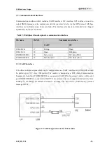
Page 23: ...CFG0 SCK 17 Pull up Open CFG1 SCS 18 Open Pull down RXD MOSI SDA 20 Data receive I2C data SDA TXD MISO SCL 19 Data transmit I2C clock SCL 3 7 1 UART Interface L50 offers multiplexed pins which can be configured as one UART interface and CFG0 SCK should be pulled up to VCC via a 10K resistor The module is designed as a DCE Data Communication Equipment Serial port TXD MISO SCL is connected to UART R...

Page 24: ...ort of host processor The UART interface does not support the RS 232 level It supports only the TTL CMOS level If the module UART interface is connected to the UART interface of a computer it is necessary to insert a level shift circuit between the module and the computer Please refer to the following figure Figure 10 RS 232 level shift circuit 3 7 2 I2C Interface L50 provides multiplex function v...

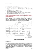
Page 25: ... Operate up to 400kbps Support Multi master I2C mode by default The default I2C master address 0x60 The default I2C slave address 0x62 The following figure is the I2C timing sequence Figure 11 I2C timing sequence The following circuit is an example of connection Quectel Preliminary ...
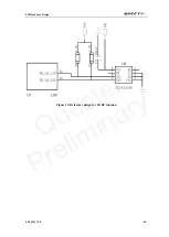
Page 26: ...GEE functionality requires that VIO RTC power supply is kept active all the time and an external 1Mbit EEPROM connected to DR_I2C bus for CGEE data storage The recommended EEPROMs are in the following table and they are verified Table 10 Recommended EEPROMs Manufacturer Part Number ST M24M01 Seiko Instruments Inc S 24CM01C Atmel AT24C1024B Note The part number which we recommend is a series part n...

Page 27: ...L50 Hardware Design L50_HD_V1 0 26 Figure 13 Reference design for CGEE function Quectel Preliminary ...

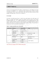
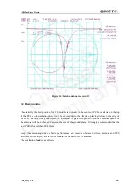
Page 28: ...pment greatly A 15 15 2 0mm patch antenna is chosen for reducing product size This antenna is specially designed for satellite reception applications And this patch antenna has excellent stability and sensitivity to consistently provide high signal reception efficiency The specification of the antenna used by L50 is described in the table below Table 12 Antenna specification for L50 module Antenna...

Page 29: ...t close to the edge of the PCB The larger the ground plane is the higher the gain is in general And the center frequency of the antenna will been changed based on the size of the ground plane It strongly recommended that the host PCB is bigger than 80 40mm Keep the antenna upside for better performance and remove obstacle between antenna and GPS satellites For example a metal cover should not be u...

Page 30: ...L50 Hardware Design L50_HD_V1 0 29 Figure 15 EVB of L50 Quectel Preliminary ...

Page 31: ... voltage If necessary voltage spikes exceeding the power supply voltage specification given in table above must be limited to values within the specified boundaries by using appropriate protection diodes 5 2 Operating Conditions Table 14 Recommended operating conditions Parameter Description Conditions Min Typ Max Unit VCC Supply voltage Voltage must stay within the min max values including voltag...

Page 32: ...es must be applied throughout the processing handing and operation of any application The ESD bearing capability of the module is listed in the following table Note that the customer should add ESD components to module pins in practical application except VCC and GND pins Table 16 The ESD endurance table Temperature 25 C Humidity 45 Pin Contact discharge Air discharge VCC GND Patch antenna 5KV 10K...

Page 33: ...0 Db Test Vibration shock 5 20Hz 0 96m2 s3 20 500Hz 0 96m2 s3 3dB oct 1hour axis no function 2423 13 1997 Test Fdb IEC 68 2 36 Fdb Test Heat test 85 C 2 hours Operational GB T 2423 1 2001 Ab IEC 68 2 1 Test Cold test 40 C 2 hours Operational GB T 2423 1 2001 Ab IEC 68 2 1 Test Heat soak 90 C 72 hours Non Operational GB T 2423 2 2001 Bb IEC 68 2 2 Test B Cold soak 45 C 72 hours Non Operational GB T...

Page 34: ... 0 33 6 Mechanical Dimensions This chapter describes the mechanical dimensions of the module 6 1 Mechanical Dimensions of the Module Figure 16 L50 Top view and Side view Unit mm Figure 17 L50 Bottom view Unit mm Quectel Preliminary ...
Page 35: ...L50 Hardware Design L50_HD_V1 0 34 6 2 Recommended Footprint Figure 18 Recommended Footprint Unit mm Quectel Preliminary ...
Page 36: ...L50 Hardware Design L50_HD_V1 0 35 6 3 Top View of the Module Figure 19 Top view of module 6 4 Bottom View of the Module Figure 20 Bottom view of module Quectel Preliminary ...
Page 37: ...ted after the first panel has been reflowed The following picture is the actual diagram which we have operated Time s 50 100 150 200 250 300 50 100 150 200 250 160 200 217 0 70s 120s 40s 60s Between 1 3 S Preheat Heating Cooling s Liquids Temperature Figure 21 Ramp soak spike reflow of furnace temperature 7 2 Moisture Sensitivity L50 is sensitive to moisture absorption To prevent L50 from permanen...

Page 38: ...ray may be damaged by high temperature heating 7 3 ESD Safe L50 module is an ESD sensitive device and should be handled carefully 7 4 Tape and Reel Figure 22 Tape and reel specification A 4 1 A 1 75 0 1 14 2 0 1 2 0 1 4 0 1 1 5 0 1 0 32 0 3 28 4 0 1 32 0 1 16 35 0 1 16 5 0 1 4 0 1 6 0 1 28 25 0 1 28 75 0 1 16 4 0 1 K K Quectel Preliminary ...

Page 39: ...L50 Hardware Design Shanghai Quectel Wireless Solutions Co Ltd Room 501 Building 13 No 99 TianZhou Road Shanghai China 200233 Tel 86 21 5108 6236 Mail info quectel com ...

Reviews: