L50 Hardware Design
L50_HD_V1.0 -21-
>1s
T>0
35ms
>1ms
400ms
400us
400us
>1ms
(Hibernate)
(Hibernate)
(FULL ON)
Invalid
Valid
Invalid
UART
WAKEUP
ON/OFF
VIO/RTC
VCC
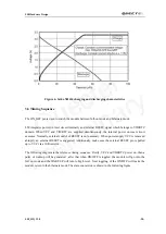
Figure 7: Turn on timing sequence of module
NOTE:
If the “ON_OFF” pin is controlled by host controller, a 1K
Ω
resistor should be inserted between
the GPIO of the controller and “ON_OFF” pin.
Figure 8: State conversion of module
Quectel
Preliminary


